Electronics 1 · Electronics Basics
#14 BJT introduction — structure, beta, and current relations
Build the NPN/PNP structure, emitter-base-collector terminals, beta current gain, and the core active-region DC model of the BJT.
Question
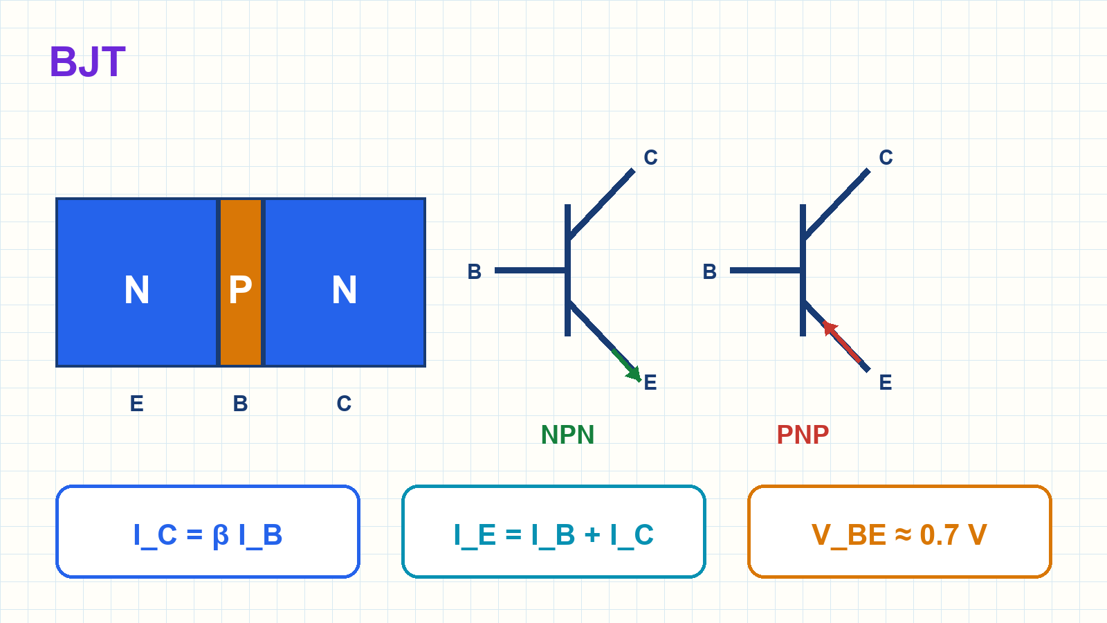
Explain the NPN and PNP structures, emitter-base-collector terminals, and core active-region DC relations of a BJT. For β = 200 and I_B = 60 μA, find I_C and I_E, and state the silicon V_BE approximation.
Written solution and narration transcript(shows the full solution)
Below are all the lines written in the notebook together with the full narration transcript.
1. Why a transistor?
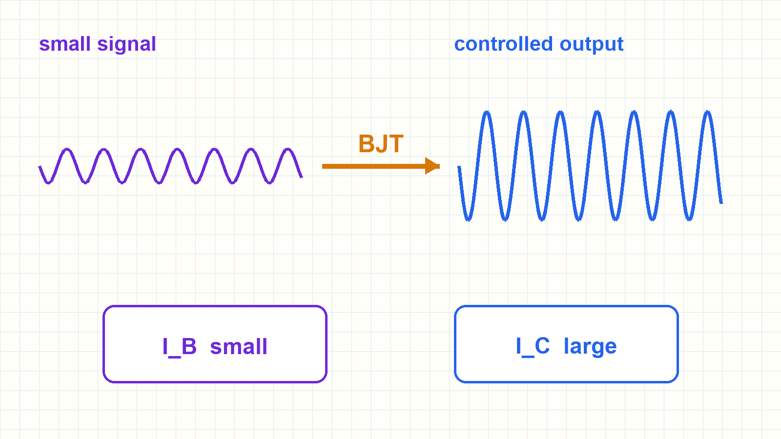
The BJT does not create energy; it controls power supplied by the source. Diode circuits shape signalsA small signal must drive a larger outputSmall IB → control of large ICA BJT controls supply powerNew goal: amplificationNarration transcript
Welcome back. Everything we have built so far, rectifiers, clippers, clampers, the Zener regulator, has one thing in common: they shape a signal, or they limit it. None of them can make it bigger. But think of a microphone. It gives you a few millivolts, and a loudspeaker needs volts. Somewhere in between, the signal has to be amplified. For that we need a completely new kind of component: one where a small current commands a much larger one. That component is the transistor. Today we meet it properly: its structure, its two families, and the simple current rules that, next time, will let us solve our very first transistor circuit down to the last volt.
2. BJT structure
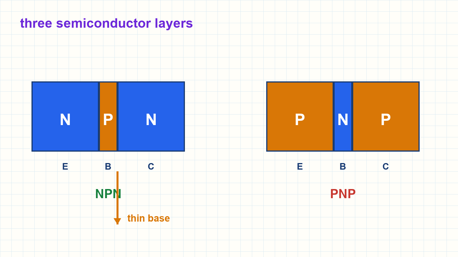
The thin middle layer is the base; the outer layers are emitter and collector. BJT = Bipolar Junction TransistorNPN: N — thin P — NE: emitter; B: base; C: collectorThin base → the key to controlPNP: P — thin N — PThe arrow is always on the emitterNarration transcript
The full name is Bipolar Junction Transistor, B J T. And the structure is simpler than the name: three layers of silicon. Take an n-type layer, then a very thin p-type layer, then another n-type layer. n, p, n. Each layer gets a terminal, and each terminal gets a name. The emitter, which emits the charge carriers. The collector, which collects them. And in the middle, the base: the thin control layer. Keep that word in mind, thin. The base being thin is the entire secret of how a transistor works. Swap the layers, p n p, and you get the second family, the pnp transistor. On the symbol, the arrow always sits on the emitter. For npn, the arrow points outward. Here is a little memory trick: n p n, Not Pointing iN. We will work with the npn, the workhorse of electronics.
3. The valve analogy
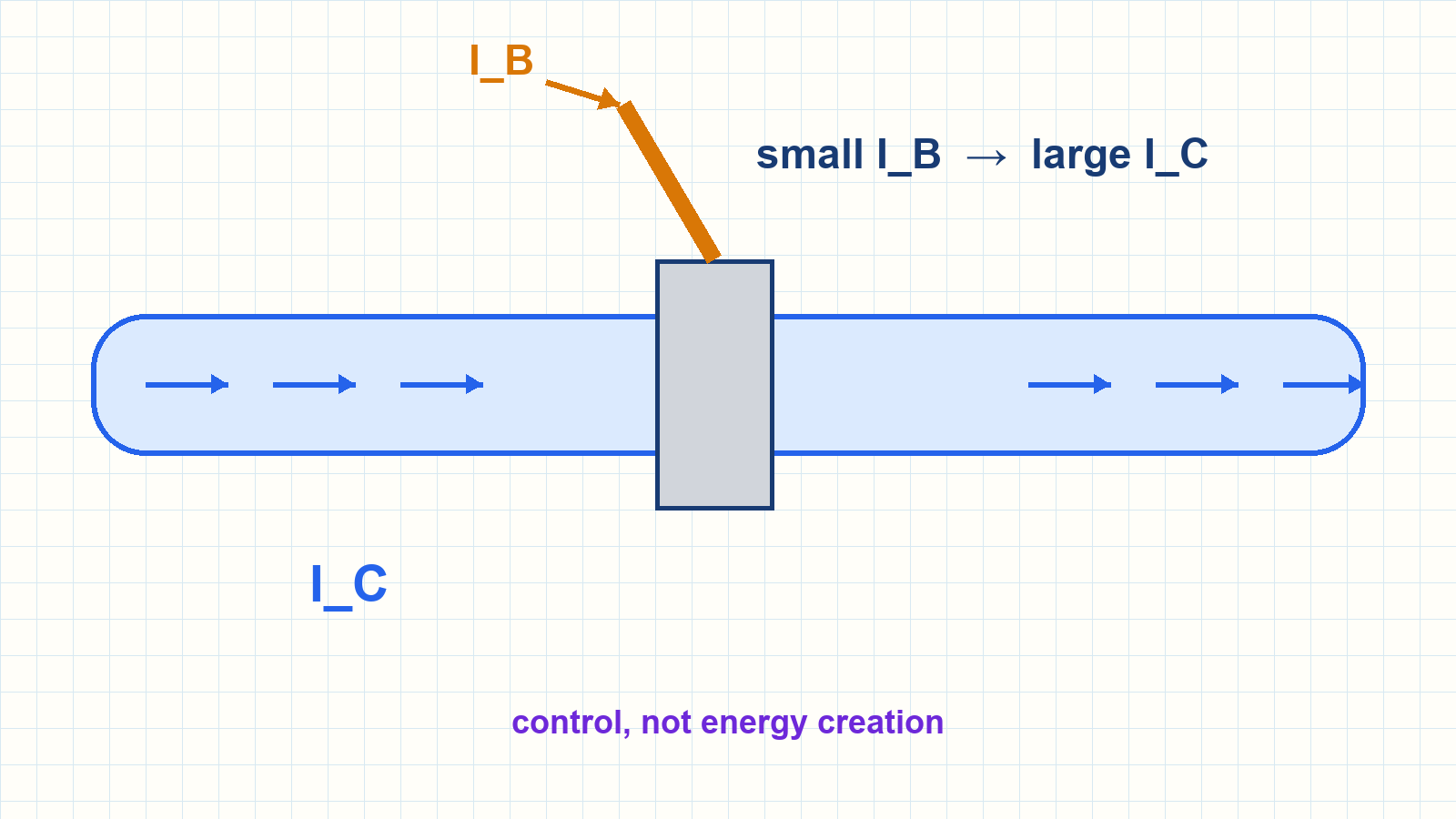
A small change in I_B controls a much larger I_C. Large pipe flow ↔ ICValve handle ↔ IBSmall motion → large current changeEnergy source: the circuit supplyCurrent gain:Narration transcript
So how does it actually behave? Picture a thick water pipe with a big flow running through it, and a valve on that pipe. The flow in the pipe is the collector current. The gentle force you apply to turn the valve handle, that is the base current. A tiny twist of the handle, and the flow changes enormously. Notice what the valve does not do: it does not create the water pressure. The pump does that, and in our circuits, the supply does that. The transistor does not create power. It controls it. And the leverage of that handle, how much flow you command per unit of effort, that is the famous beta.
4. Current relations
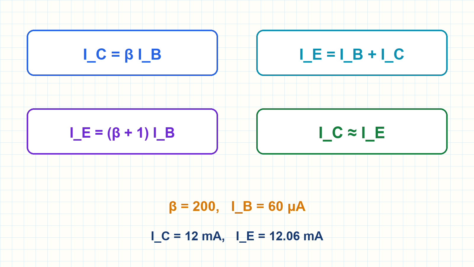
I_C = βI_B, I_E = I_B + I_C, and the I_C approximately I_E result. IC = 12 mAIE = 12.06 mANarration transcript
Let us turn that picture into equations, slowly. Beta is the current gain: the collector current is beta times the base current. I sub C equals beta times I sub B. Typical betas run from fifty up to a few hundred, so the collector current is fifty to a few hundred times larger than the base current. Now, where do these currents go? Into the device flow I sub B and I sub C, and everything that flows in must flow out, through the emitter. So I sub E equals I sub B plus I sub C. That is just Kirchhoff's current law. Substitute I sub C: I sub E equals I sub B plus beta times I sub B, which is beta plus one, times I sub B. Let us feel these with numbers. Say beta is two hundred, and the base current is sixty microamps. The collector current: two hundred times sixty is twelve thousand. Twelve thousand microamps. Slide the decimal three places: twelve milliamps. The emitter current: two hundred one times sixty is twelve thousand sixty microamps, which is 12.06 milliamps. Now compare them. Twelve, and 12.06. Almost identical. And that gives us a rule we will use constantly: I sub C is approximately equal to I sub E. The base current is so tiny that it barely shows up in the sum.
5. Two golden models
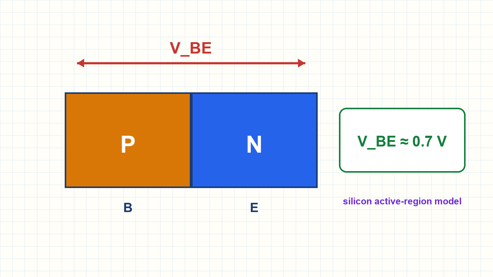
The active-region approximation uses V_BE approximately 0.7 V. The B-E path is a P-N junctionSilicon, forward biased, active regionCapital symbols → DC operating valuesLowercase symbols → AC signal valuesNarration transcript
Before we touch a real circuit, I want to hand you the two golden facts that unlock every D C analysis. Fact one. Look closely at the base to emitter junction: p-type material against n-type material. That is a p n junction. That is literally a diode, the very first component of this series. And when it is forward biased, you already know what it drops: 0.7 volts. So V sub B E equals 0.7 volts. Always our entry key. Fact two, you have already met: I sub C equals beta times I sub B. One small notation note. Capital letters, like I sub B and V sub C E, mean D C values. Lowercase letters mean A C signals. Today is pure D C, so capitals everywhere.
6. Method summary
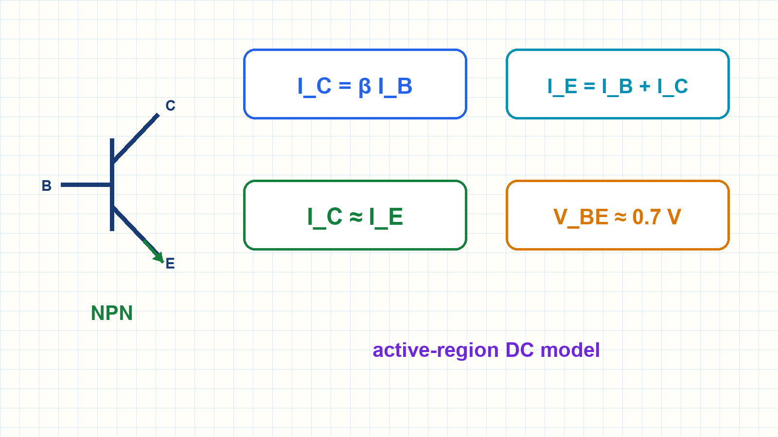
These models unlock the fixed-bias analysis in the next lesson. 1) BJT: emitter — thin base — collector2) NPN and PNP are the two families3) Small IB → β times larger IC4) Apply IE = IB + IC5) In active region use VBE ≈ 0.7 VNext step: the fixed-bias circuitNarration transcript
Let us gather what we have. The Bipolar Junction Transistor: three layers of silicon, emitter, thin base, collector, in two families, npn and pnp. It behaves like a valve: a tiny base current commands a collector current beta times larger. The bookkeeping is Kirchhoff: I sub E equals I sub B plus I sub C, and because the base share is so tiny, I sub C is approximately I sub E. And carry the two golden facts with you everywhere: V sub B E is 0.7 volts, and I sub C is beta times I sub B. Next time, we put the transistor into its first real circuit, the fixed-bias circuit, and we solve it completely: every current, every voltage, down to the last volt. See you there.
Source video: Electronics Basics #14 | What Is a Transistor? BJT Basics: npn vs pnp, Beta and the Valve Analogy (6:03)