Electronics 1 · Electronics Basics
#21 JFET and Shockley’s equation — calculate, then check
Question
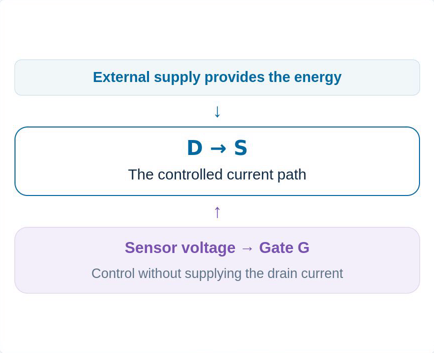
How can a small sensor voltage control current without supplying it? For an n-channel JFET with I_DSS=8 mA, V_P=−4 V, V_GS=−2 V and V_DS=5 V, calculate the drain current and check the model assumptions. These are teaching values, not a real-part specification.
Written solution and narration transcript(shows the full solution)
Below are all the lines written in the notebook together with the full narration transcript.
1. The goal: control current with voltage
Sensor: small voltage, limited currentGoal: voltage controls a larger currentControl input ≠ drain-to-source current pathNarration transcript
Imagine a sensor that gives us a small voltage, but cannot supply much current. Our goal is to let that voltage control a larger current without drawing much current from the sensor itself. Look at the two paths on the screen: a control input at the side, and a current path from drain to source. They do different jobs.
2. The goal: control current with voltage
Original same-language video illustration; not a commercial device specification. Junction field-effect transistor (JFET)Picture → equation → calculation → physical checkEnergy comes from the external supplyNarration transcript
Today we meet the junction field-effect transistor, or J FET. By the end, you will be able to find its drain current from a gate voltage, and decide whether your answer makes physical sense. We will begin with the picture, then build the equation, then calculate a simple example. The energy in the controlled current comes from the external supply, not from the control signal.
3. Three terminals, a different control mechanism
G: gate · D: drain · S: sourceN-channel: conceptual cutaway, not to scaleElectric field changes depletion; no mechanical squeezingNarration transcript
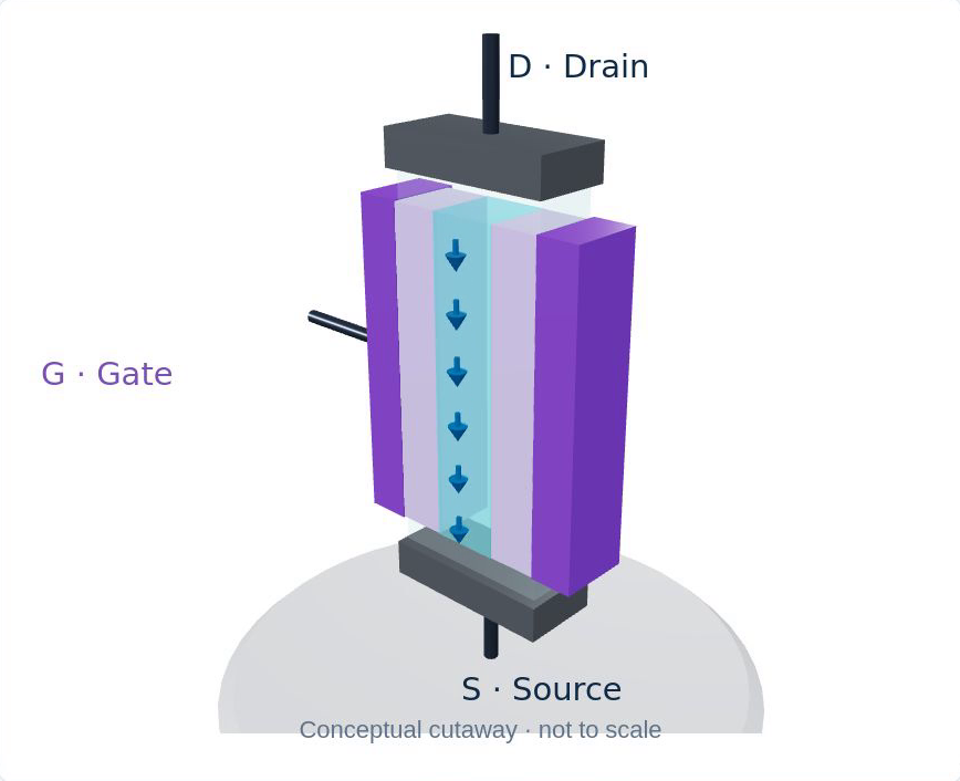
There are three terminals. G means gate, D means drain, and S means source. In the n-channel device shown here, the gate controls a conducting channel. Our cutaway is a conceptual model, not a drawing of a particular commercial part. The gate material does not mechanically squeeze the channel; an electric field changes the depleted region inside the semiconductor.
4. Three terminals, a different control mechanism
Conventional current: D → SElectron motion: S → DBlue: current · Purple: controlling gateNarration transcript
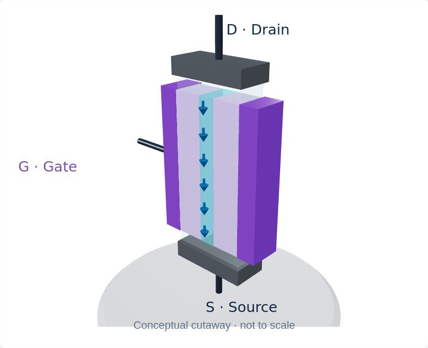
The conventional drain current enters at D and leaves at S. Electrons in this n-channel device travel the other way, from source to drain. We will show conventional current with the blue arrows, so we do not switch directions halfway through the lesson. The purple region belongs to the gate, which controls the channel from the side.
5. Three terminals, a different control mechanism
Original same-language video illustration; not a commercial device specification. Earlier BJT approximation:JFET first approximation:IG ≈ 0 does not imply ID ≈ 0Narration transcript
In our earlier BJT bias calculations, we used collector current equal to beta times base current. A base current was part of the calculation. For the J FET, the first approximation is different: the gate current is approximately zero. Do not conclude that the drain current must also be zero. The gate controls a separate current path; it does not have to supply that current.
6. Why almost no gate current?
Gate-channel PN junction is reverse-biasedReal leakage: approximately zero, not exactly zeroJFET junction gate ≠ MOSFET oxide gateNarration transcript
Why is the gate current so small? The gate forms a P N junction with the channel. In normal n-channel operation we reverse-bias that junction. There is still a small leakage current in a real device, so approximately zero is more honest than exactly zero. This is a junction gate, not the insulated oxide gate of a MOSFET.
7. Why almost no gate current?
Current conservation is unchangedNarration transcript
Now apply current conservation. The current leaving the source equals the drain current plus the gate current entering the device. Replace the gate current by approximately zero, and the source current is approximately equal to the drain current. That is one less unknown to worry about. This is the same conservation law you already used with a BJT; only the size of the control-terminal current has changed.
8. Why almost no gate current?
Original same-language video illustration; not a commercial device specification. VGS is variable; do not substitute 0.7 VNarration transcript
Next, read the voltage correctly. V G S means gate potential minus source potential: first letter minus second letter. If the gate is at zero volts and the source is at two volts, zero minus two gives negative two volts. Unlike the fixed zero-point-seven-volt approximation we used for a silicon BJT junction, the J FET gate-source voltage is not a fixed constant.
9. Two landmarks and Shockley’s equation
IDSS: ID at VGS = 0, with enough VDS for saturationSigned n-channel cutoff parameter: VP = VGS(off) < 0Narration transcript
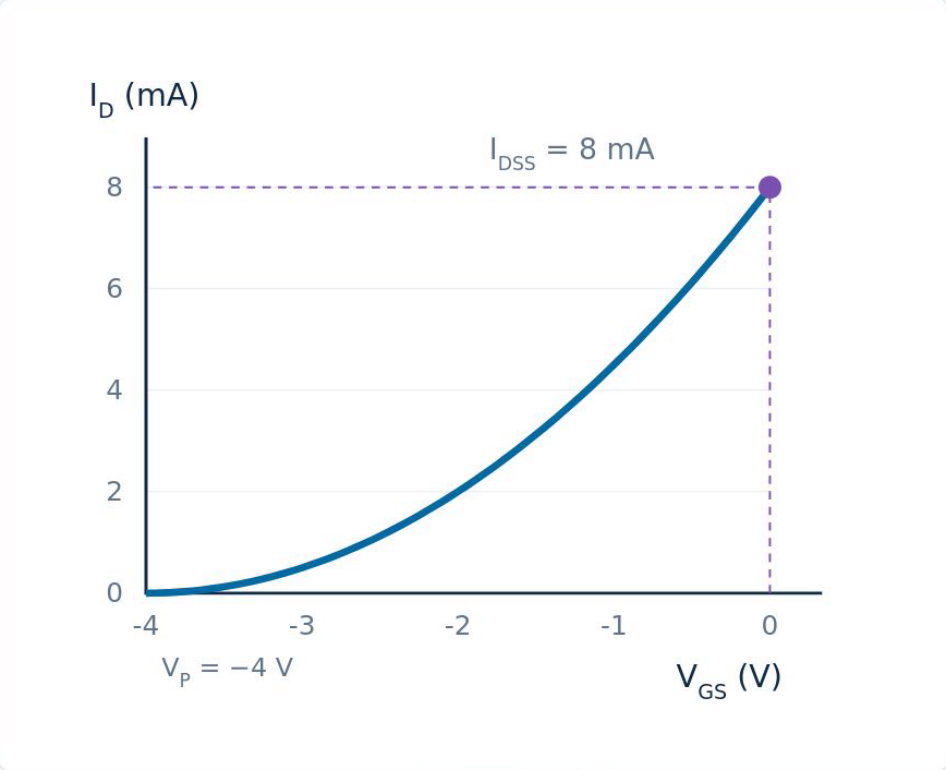
Two device parameters give us our landmarks. I D S S is the drain current at zero gate-source voltage, with enough drain-source voltage for saturation operation. It is not the current at every possible drain voltage. The other parameter is V G S off: the negative gate-source voltage that brings an n-channel device close to cutoff. In our source notes, this signed voltage is called V P.
10. Two landmarks and Shockley’s equation
Ratio → subtract from 1 → square → multiply by IDSSV/V has no unitNarration transcript
Shockley's equation connects the two landmarks with a curve. Drain current equals I D S S, multiplied by the square of one minus the ratio of gate-source voltage to V P. Do not let the subscripts distract you. We are taking a voltage ratio, subtracting it from one, squaring the result, and multiplying by a current. The ratio has no unit because volts divide by volts.
11. Two landmarks and Shockley’s equation
Ideal cutoff:Narration transcript
Test the endpoints before trusting a formula. At zero gate-source voltage, zero divided by V P is zero. One minus zero is one, and one squared is one. So the drain current equals I D S S. At cutoff, gate-source voltage equals V P. Their ratio is one; one minus one is zero; zero squared is zero. The ideal model then gives zero drain current.
12. Work it out: every step
Teaching example; not a device specificationVDS = 5 V · Find ID, then check the regionNarration transcript
Let us add a numerical example to make that concrete. These are teaching values, not a specification for a particular part. I D S S is eight milliamps, V P is negative four volts, and gate-source voltage is negative two volts. We also choose five volts from drain to source. Our target is the drain current, and afterward we will check the operating region.
13. Work it out: every step
Both minus signs matter; the ratio is positiveNarration transcript
Begin with the ratio inside the brackets. Negative two volts divided by negative four volts is positive one half, or zero point five. The two negative signs cancel. This is where a sign error can quietly make your answer much too large. Keep both minus signs visible until you have actually performed the division.
14. Work it out: every step
0.5 × 0.5Half the voltage range does not mean half the currentNarration transcript
Now do the subtraction: one minus zero point five equals zero point five. We are not finished. The brackets are squared, so multiply zero point five by zero point five. That gives zero point two five, one quarter. Halfway across the allowed voltage range does not mean half the current, because this relationship is curved, not a straight line.
15. Work it out: every step
The current unit comes from IDSSNarration transcript
Finally multiply eight milliamps by one quarter. Eight times zero point two five equals two, so the drain current is two milliamps. The bracket had no unit; the milliamps came from I D S S. In amperes this is zero point zero zero two. Because gate current is negligible, source current is also approximately two milliamps.
16. Work it out: every step
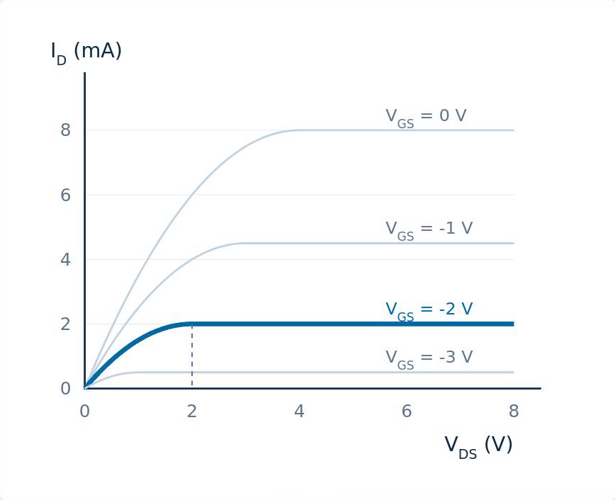
Original same-language video illustration; not a commercial device specification. Sanity check:18 [mA] would signal a likely sign errorMagnitude alone does not verify the operating regionNarration transcript
Does that size make sense? With the gate moved from zero toward cutoff, current should decrease from eight milliamps toward zero. Two milliamps lies between those limits. If you found eighteen milliamps for these inputs, stop and inspect the signs before moving on. A reasonable magnitude is a useful check, but we still have to check the region.
17. Pinch-off is not the same as cutoff
Pinch-off near drain: current continues on a plateauCutoff: sufficiently negative gate voltage suppresses currentCheck the book’s voltage definition and sign conventionNarration transcript
Here is an important language trap. Pinch-off near the drain end marks the start of approximately constant-current operation. It does not mean the drain current has stopped. Cutoff is the different situation where a sufficiently negative gate voltage suppresses the current nearly to zero. Textbooks sometimes use the name pinch-off voltage for the cutoff parameter too, so always check which voltage and sign convention they mean.
18. Pinch-off is not the same as cutoff
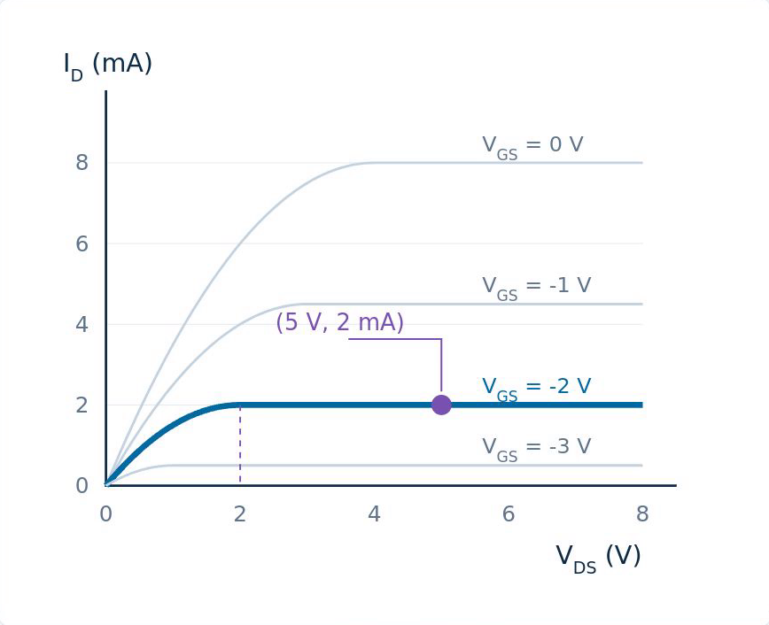
Original same-language video illustration; not a commercial device specification. Model: VP ≤ VGS ≤ 0; below breakdownSaturation threshold:Narration transcript
Our simple Shockley calculation describes the saturation region, below breakdown, with gate voltage between V P and zero. For this signed n-channel convention, saturation begins approximately when drain-source voltage reaches gate-source voltage minus V P. In our example that is negative two minus negative four. Subtracting a negative adds four: negative two plus four equals positive two volts.
19. Pinch-off is not the same as cutoff
5 V > 2 V: saturation check passes, below breakdown assumedOperating point:Small VDS: ohmic region; saturation formula is not validNarration transcript
We chose five volts across drain and source. Five is greater than two, so the ideal saturation check passes, assuming five volts is safely below the actual device's breakdown rating. Look at the graph: the point is on the plateau at two milliamps. At a very small drain voltage, the device would be in the ohmic region and the same saturation-current formula would not give its actual drain current.
20. The calculator does not know the device
Bias relation + squared Shockley equation → two algebraic rootsA calculator does not check device physicsNarration transcript
Our original notes finish with a warning about quadratic equations. In later bias circuits, gate-source voltage can depend on the unknown drain current. Substituting that circuit relation into the squared Shockley equation can produce a quadratic, with two mathematical roots. A calculator can find both, but it cannot tell you which root describes a working transistor.
21. The calculator does not know the device
x = (−b ± √(b2 − 4ac))/(2a)For each root: gate voltage → allowed interval → drain regionPositive or smaller is not a physical selection ruleNarration transcript
The general roots are negative b, plus or minus the square root of b squared minus four a c, all divided by two a. We do not need to solve a full bias circuit today. The habit we need now is this: for each candidate current, calculate its corresponding gate voltage, check the permitted gate-voltage interval, and then check the drain-voltage region. Do not select a root merely because it is positive, or because it is the smaller one.
22. The calculator does not know the device
Try VGS = −6 V: outside the VP = −4 V cutoff boundBare algebra:Algebra predicts 2 [mA] again — not a valid operating resultReject extrapolation: the device is near cutoffNarration transcript
For a quick demonstration of the danger, take our same parameters but try a gate voltage of negative six volts. That is beyond the negative-four-volt cutoff. The bare algebra gives negative six over negative four equals one point five; one minus one point five equals negative zero point five; squaring gives one quarter. It then predicts two milliamps again. The algebra ran, but its operating assumptions failed. The physical device is near cutoff, not back on the same two-milliamp point.
23. Your JFET analysis checklist
Goal answered: voltage controls current with IG ≈ 0Know G/D/S; IS ≈ ID; VGS is not fixed8 [mA], −4 V, −2 V → ID = 2 [mA] in saturationNarration transcript
Let us return to our goal. A gate-source voltage controls the channel current while drawing very little steady gate current. We named gate, drain and source; used gate current approximately zero to get source current approximately equal to drain current; and replaced the fixed-junction-voltage habit with a variable gate-source voltage. For eight milliamps and negative four volts as device parameters, a negative-two-volt control gave two milliamps in saturation.
24. Your JFET analysis checklist
Signs → Shockley → physical checksNext: find VGS from the fixed-bias circuitNarration transcript
Keep this order: voltage signs first, Shockley's equation second, physical checks last. The number is not finished until its assumptions pass. Next time we put the J FET into a fixed-bias circuit and find the gate voltage from the actual connections, instead of receiving it as a given. That is where this small set of rules becomes a complete circuit-analysis method.
Source video: Electronics Basics #21 | JFET & Shockley’s Equation — Step by Step (11:25)