Electronics 1 · Electronics Basics
#26 Depletion MOSFET divider bias — test the device domain
Question
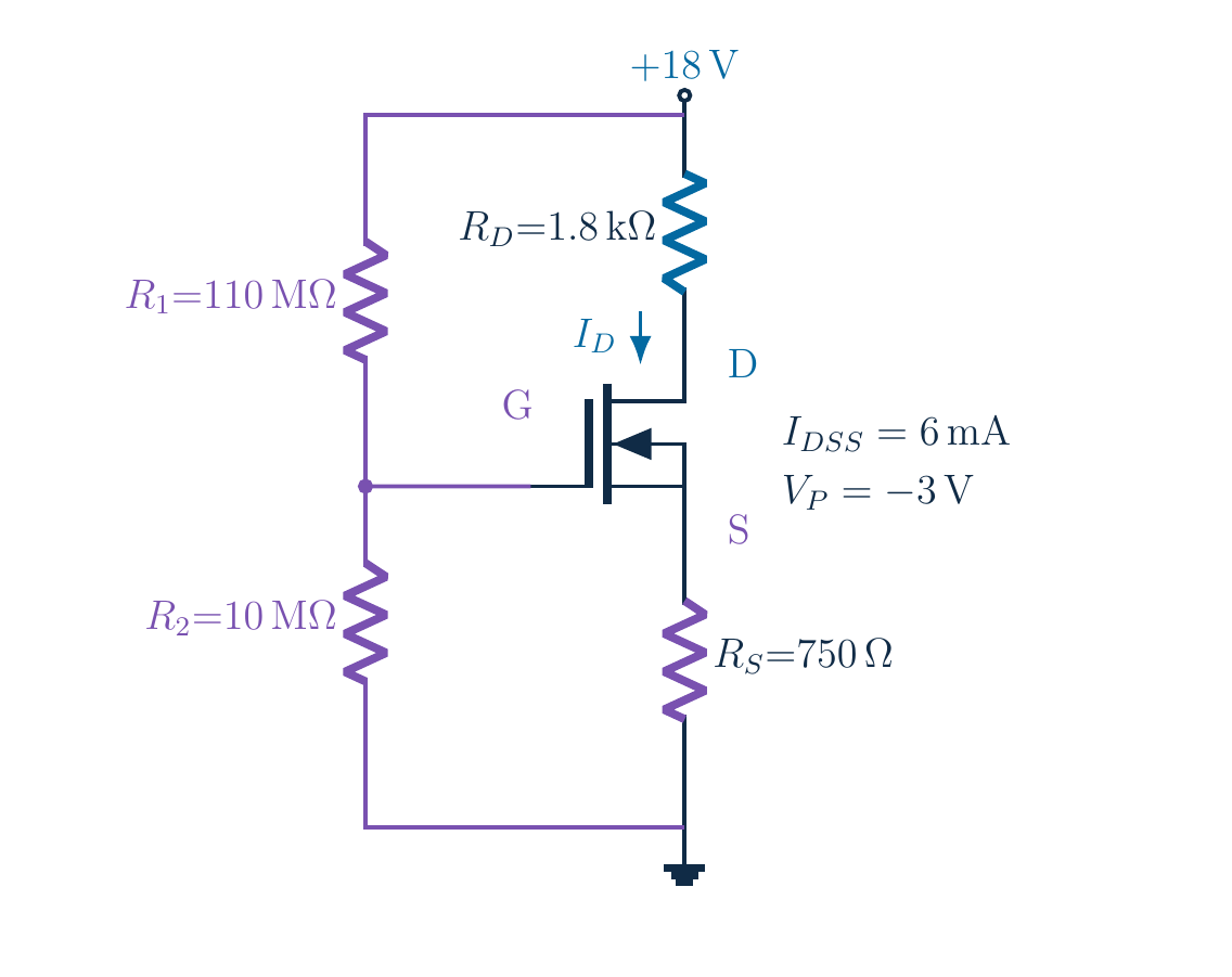
Find the no-signal operating point of the 18 V depletion-MOSFET circuit. Use R_D=1.8 kΩ, R_S=0.75 kΩ, upper/lower divider 110 MΩ/10 MΩ, I_DSS=6 mA and V_P=−3 V. Why must we not copy the JFET positive-gate rejection rule?
Written solution and narration transcript(shows the full solution)
Below are all the lines written in the notebook together with the full narration transcript.
1. The goal: find the current before applying a signal
Goal: inspect the whole 18 V circuit firstQ: ID, VGS and VDS before any signalNarration transcript
Before solving anything, look at the complete circuit. An eighteen-volt supply feeds a transistor through a drain resistor. A second resistor lifts its source above ground, while a divider sets its gate voltage. Our goal is practical: how much current flows before any signal is applied, and what voltages appear across the transistor? We need the drain current, the gate-source voltage, and the drain-source voltage. The letter Q means the quiescent, or no-signal, operating point.
2. The goal: find the current before applying a signal
Divider: upper 110 MΩ; lower 10 MΩPreserve supplied megaohm values; state ideal assumptionsNarration transcript
Read the values from the original lesson forty-one circuit. The drain resistor is one point eight kilohms. The source resistor is seven hundred fifty ohms, or zero point seven five kilohms. The upper divider resistor is one hundred ten megohms; the lower is ten megohms. I D S S is six milliamps, and V P is negative three volts. Notice the megaohm units on the divider. We preserve these supplied values rather than silently replacing them with a more typical practical design.
3. An insulated gate and a normally-on channel
N-channel depletion MOSFET; insulated gate; IG≈0VGS=0: already conducting; saturation current IDSSCutoff at VP=−3 V; solid-channel symbolNarration transcript
This is an n-channel depletion-type MOSFET, not a J FET and not an enhancement-only MOSFET. Its gate is insulated from the channel. In our ideal direct-current model the gate current is negligible. The channel already conducts at zero gate-source voltage: in saturation, its current then equals I D S S. A sufficiently negative control voltage depletes the channel and turns it off. Here that cutoff boundary is negative three volts. The solid channel in the schematic identifies the depletion-type symbol.
4. An insulated gate and a normally-on channel
Depletion MOSFET can also accept positive VGSPositive bias is not an automatic invalid-root testModel domain: VGS≥VP; actual device ratings still applyNarration transcript
There is an important difference from the gate-range restriction used for an n-channel J FET. A depletion MOSFET can also operate with a positive gate-source voltage. Within the saturation model, a negative voltage above cutoff reduces current below I D S S, while a positive voltage increases it above I D S S. Positive voltage is not automatically an invalid root. The model's conduction boundary is V G S greater than or equal to V P; actual oxide, voltage, and power ratings still limit a real device.
5. Find the gate voltage, then the control voltage
IG≈0 → approximately unloaded dividerVG = 18 × 10/(110+10) V; exclude RSNarration transcript
Start with the part we can solve without knowing the drain current. Since the ideal gate takes essentially no current, it does not load the divider. Gate voltage relative to ground equals the supply multiplied by the lower resistance divided by the total resistance. The upper and lower values are both in megohms, so that common unit cancels in the ratio. Substitute eighteen times ten divided by one hundred ten plus ten. Do not use the source resistor as part of this divider.
6. Find the gate voltage, then the control voltage
VG=1.5 V, referenced to ground, not sourceIdiv=18 V/(120 MΩ)=150 nALeakage can matter; this is an ideal textbook modelNarration transcript
The divider gives one point five volts at the gate. This is a gate-to-ground voltage, not yet the gate-source voltage. There is also a useful modeling warning. The total divider resistance is one hundred twenty megohms, so the divider current is only one hundred fifty nanoamps. Leakage and contamination could matter in actual hardware. For this supplied textbook problem we explicitly retain the negligible-leakage assumption, rather than confusing an ideal calculation with a complete real-world design.
7. Find the gate voltage, then the control voltage
Let x=ID/(1 [mA])Narration transcript
The source voltage is not zero because current flows through the source resistor. With negligible gate current, source and drain currents are equal. Write source voltage as drain current times source resistance, then subtract it from the gate voltage. To keep the algebra readable, let x be the numerical value of drain current in milliamps. The source voltage is then zero point seven five x volts, and the gate-source voltage is one point five minus zero point seven five x volts. Do not substitute x in amperes into this particular expression.
8. One unknown links the circuit and the device
VP=−3 V → factor 1+VGS/(3 V)Check conduction domain and saturation after solvingNarration transcript
The second relation comes from the device. In the ideal saturation model, drain current equals I D S S multiplied by one minus V G S divided by V P, all squared. Because V P is negative three volts, the term becomes one plus V G S divided by three volts. The plus sign is important. This is a model for the conducting saturation region, not an equation to apply blindly below cutoff. After finding a candidate, we must check both the gate-voltage domain and the drain-source saturation condition.
9. One unknown links the circuit and the device
Divide both terms: 0.5−0.25xNarration transcript
Substitute the circuit expression for V G S into the device equation. We get x equals six times the square of one plus the quantity one point five minus zero point seven five x, divided by three. Divide both terms inside that quantity by three. One point five becomes zero point five, and zero point seven five x becomes zero point two five x. Combining the constant terms leaves one point five minus zero point two five x inside the square. We now have one equation in one unknown.
10. One unknown links the circuit and the device
Multiply by 6, then move xNarration transcript
Expand the square carefully. The first term is two point two five. The cross term is negative zero point seven five x, because it is twice the product of the two terms with a minus sign. The last term is zero point zero six two five x squared. Multiply everything by six, then move the x on the left to the right. The final polynomial is zero point three seven five x squared minus five point five x plus thirteen point five equals zero. Keeping the cross term prevents a common wrong answer.
11. Two algebraic roots, one physical candidate
Candidate currents: 3.117 [mA] and 11.550 [mA]; test bothNarration transcript
Apply the quadratic formula. The coefficient a is zero point three seven five, b is negative five point five, and c is thirteen point five. The discriminant is ten. Therefore x equals five point five plus or minus the square root of ten, divided by zero point seven five. The two numerical currents are approximately three point one one seven and eleven point five five zero milliamps. Write down both. A calculator has solved the polynomial; it has not decided whether either current can actually occur in this circuit.
12. Two algebraic roots, one physical candidate
Large root → VGS≈−7.162 V−7.162 V < −3 V: reject below cutoffRejection follows domain, not a generic root-size ruleNarration transcript
Test the larger root first. Substitute its unrounded value into the circuit relation for gate-source voltage. The result is approximately negative seven point one six two volts. That is below the negative-three-volt cutoff boundary, so we reject this root. Squaring an expression can produce a positive number even when the unsquared channel-control term has the wrong sign. This rejection is not a rule that the bigger root is always wrong; it comes from the actual operating domain of the device model.
13. Two algebraic roots, one physical candidate
Small root → VGS≈−0.838 VAbove cutoff; ID<IDSS; source above positive gateGate-domain check passes; saturation still pendingNarration transcript
Now test the smaller root using its unrounded value. The gate-source voltage is approximately negative zero point eight three eight volts. It lies above cutoff and below zero, so the current being below six milliamps is consistent with depletion operation. The gate is positive relative to ground, but the source is higher still. This candidate passes the gate-domain check. Do not call the analysis complete yet: we have used a saturation equation, so we still need to prove that the drain-source voltage is sufficient for saturation.
14. Calculate the voltages and test saturation
VS=0.75 ID ≈ 2.338 V (ID in [mA])Both node voltages referenced to groundNarration transcript
Calculate the two node voltages separately to make their references clear. Source voltage is current times zero point seven five kilohms, giving about two point three three eight volts above ground. Drain voltage is the supply minus the drop across the one point eight kilohm drain resistor. Using the unrounded current gives approximately twelve point three eight nine volts. We now know where gate, source, and drain sit relative to ground. The control voltage is gate minus source; the channel voltage will be drain minus source.
15. Calculate the voltages and test saturation
Use unrounded current; methods agreeNarration transcript
Subtract the source voltage from the drain voltage. Equivalently, walk around the entire drain-source loop: the supply equals the drain-resistor drop, the transistor voltage, and the source-resistor drop. That gives V D S equals eighteen minus drain current times the sum of one point eight and zero point seven five kilohms. With the unrounded current the result is approximately ten point zero five two volts. The two methods agree. Small differences from subtracting displayed rounded numbers are just rounding, not a different operating point.
16. Calculate the voltages and test saturation
Saturation:Boundary ≈ 2.162 V10.052 V > 2.162 V: accepted in the ideal modelNarration transcript
For this depletion MOSFET, the textbook parameter V P is the negative threshold of our ideal model. Saturation requires V D S to be at least V G S minus V P. Subtracting negative three from negative zero point eight three eight gives a boundary of about two point one six two volts. The available channel voltage is about ten point zero five two volts, so this candidate passes the saturation check. We can now accept the operating point within the stated model, assuming the real device has appropriate voltage and power ratings.
17. Calculate the voltages and test saturation
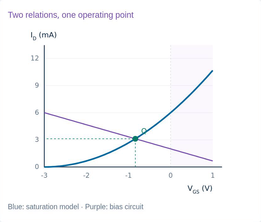
Original lesson graph; ideal DC model. Unrounded loop voltage sum = 18 VDisplayed sum 18.001 V: rounding onlyDevice substitution returns ID≈3.117 [mA]Narration transcript
Perform two final checks instead of trusting only the quadratic formula. First add the drain-resistor drop, transistor voltage, and source-resistor drop. The unrounded values return eighteen volts. The three-decimal numbers on screen add to eighteen point zero zero one, a harmless rounding difference. Second, substitute the unrounded gate-source voltage back into the square-law device equation. It returns the same three point one one seven milliamp current. The circuit equation and the device equation therefore describe the same accepted operating point.
18. The checked operating point and a reusable method
Transfer curve extends into positive VGSCircuit line:Q: ID≈3.117 [mA]; VGS≈−0.838 V; saturation checkedNarration transcript
The graph makes the answer visible. The blue curve is the saturation transfer model. Unlike the restricted J FET plot, it continues into positive gate-source voltage. The purple line represents the source resistor and the fixed gate potential: current equals gate voltage minus gate-source voltage, divided by source resistance. Their intersection is Q, with approximately three point one one seven milliamps and negative zero point eight three eight volts. Our separate drain-voltage calculation confirmed that this graphical candidate really lies in saturation.
19. The checked operating point and a reusable method
Identify device → divider → source feedback → equationTest roots, terminal voltages and saturationNormally on; either bias sign allowed within device ratingsNarration transcript
Take away the method, not just the answer. Begin with the overall goal and identify the transistor type. Find the unloaded divider voltage, express the source voltage through current, and combine that circuit relation with the device equation. Test each root against the physical domain, then calculate the terminal voltages and verify saturation. Remember the new idea: a depletion MOSFET is normally on and can accept either sign of gate-source voltage within its ratings. In this particular circuit, source feedback leads to the negative-bias operating point we have just checked.
Source video: Electronics Basics #26 | Depletion MOSFET DC Analysis: Voltage-Divider Bias (12:26)