Electronics 1 · Electronics Basics
#27 Depletion MOSFET self-bias — grounded gate is not zero V_GS
Question
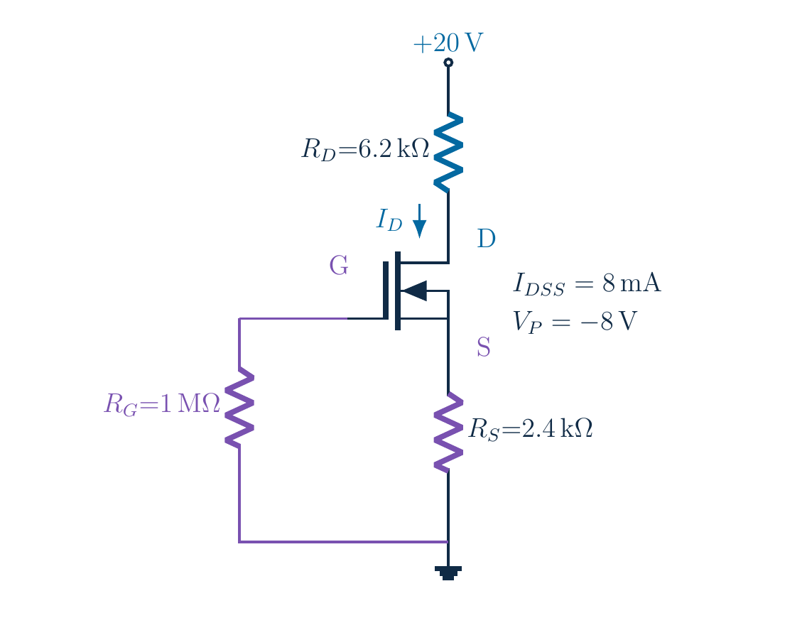
Does a grounded gate force I_D=I_DSS? Find Q for V_DD=20 V, R_D=6.2 kΩ, R_S=2.4 kΩ, R_G=1 MΩ, I_DSS=8 mA and V_P=−8 V. Check both roots even though both are below I_DSS.
Written solution and narration transcript(shows the full solution)
Below are all the lines written in the notebook together with the full narration transcript.
1. The goal: understand what a grounded gate really sets
Whole circuit: gate and source have different paths to groundGrounded gate does not imply VGS=0Find Q, then check the assumed saturation modelNarration transcript
Look at the whole circuit first. The gate reaches ground through a large resistor, but the source reaches ground through a different resistor carrying the transistor current. Does a grounded gate mean zero gate-source voltage and a current equal to I D S S? Not necessarily. Our goal is to find the actual no-signal operating point. We will calculate current and terminal voltages, then check whether the saturation model we used is self-consistent.
2. The goal: understand what a grounded gate really sets
RG=1 MΩ connects gate to groundDepletion MOSFET: IDSS=8 [mA]; VP=−8 V; body tied to sourceNarration transcript
Preserve the original lesson forty-two values. The supply is twenty volts, the drain resistor six point two kilohms, and the source resistor two point four kilohms. The gate resistor is one megohm and connects to ground, not to the positive supply. The n-channel depletion MOSFET has I D S S equal to eight milliamps and V P equal to negative eight volts. Its body is tied to the source in the symbol. These connections define a self-bias circuit.
3. The source resistor creates the control voltage
VS=ID RS, generally nonzeroVGS=−ID RS; no negative supply neededNarration transcript
In the ideal model, gate leakage is negligible. Therefore the voltage drop across the one-megohm gate resistor is approximately zero, and the gate is at ground potential. The source resistor carries the drain current, so its voltage is not generally zero. Source voltage equals drain current times source resistance. Subtract source voltage from gate voltage: V G S equals negative I D R S. The resistor in the source branch creates a negative control voltage without a separate negative gate supply.
4. The source resistor creates the control voltage
ID rises → source rises → VGS more negativeNegative feedback, not an ideal current sourceNarration transcript
Let x be the numerical drain current in milliamps. Multiplying milliamps by kilohms gives volts, so source voltage is two point four x volts and gate-source voltage is negative two point four x volts. This is the circuit relation, valid before we know the numerical current. If current tries to rise, the source rises and V G S becomes more negative, opposing that rise. This feedback helps stabilize the bias; it does not make an ideal constant-current source.
5. Combine the circuit relation with the device model
Substitute VGS=−2.4x VNarration transcript
Use the ideal square-law saturation model: I D equals I D S S times the square of one minus V G S divided by V P. Since V P is negative eight volts, the expression becomes one plus V G S divided by eight volts. Substitute negative two point four x for V G S. Dividing two point four by eight gives zero point three, leaving one minus zero point three x inside the square. The resulting equation contains only x.
6. Combine the circuit relation with the device model
x=8−4.8x+0.72x2; move xNarration transcript
Expand the square as one minus zero point six x plus zero point zero nine x squared. Remember the factor of two in the cross term. Multiply by eight to obtain x equals eight minus four point eight x plus zero point seven two x squared. Move the x from the left to the right. The final polynomial is zero point seven two x squared minus five point eight x plus eight equals zero. The extra negative x is why the coefficient is five point eight rather than four point eight.
7. Check both roots, not just their current magnitudes
Candidates: ID≈1.767 [mA] and 6.289 [mA]Both below IDSS: still test each gate voltageNarration transcript
The quadratic formula gives a discriminant of ten point six. The numerator is five point eight plus or minus the square root of ten point six, and the denominator is one point four four. The roots are approximately one point seven six seven and six point two eight nine milliamps. Both happen to be less than the eight-milliamp I D S S value. That does not make them both valid. We must check the gate-source voltage produced by each current in the actual circuit.
8. Check both roots, not just their current magnitudes
Large root → VGS≈−15.093 V−15.093 V < −8 V: outside conducting domainSquaring hides the sign; ID<IDSS alone is insufficientNarration transcript
For the larger root, multiply the unrounded current by negative two point four. The gate-source voltage would be approximately negative fifteen point zero nine three volts. This is below the negative-eight-volt cutoff boundary, so reject this candidate. The conducting square-law model is being continued outside its valid domain. Squaring masks the sign problem and creates a positive algebraic current. Notice why checking only that current is less than I D S S would have accepted a physically invalid solution.
9. Check both roots, not just their current magnitudes
Small root:Above cutoff; positive source, negative self-biasGate domain passed; drain-voltage check remainsNarration transcript
For the smaller root, use the unrounded current of about one point seven six six eight three milliamps. The gate-source voltage is approximately negative four point two four zero volts. This lies above cutoff and below zero, as expected for this grounded-gate self-bias circuit. The corresponding source voltage is positive. We have a valid gate-domain candidate, but we still need the drain-source voltage before accepting the assumed saturation region. A correct current equation is only one part of a complete bias analysis.
10. Calculate the node and terminal-pair voltages
Source not grounded → VDS=VD−VSNarration transcript
Calculate the node voltages relative to ground. The source voltage is drain current times two point four kilohms, or approximately four point two four zero volts. The drain voltage is twenty volts minus the current times six point two kilohms, giving approximately nine point zero four six volts. The source is not ground, so the drain voltage alone is not the voltage across the transistor. To get the transistor's drain-source voltage, subtract the source voltage from the drain voltage.
11. Calculate the node and terminal-pair voltages
VDS=20−8.6 ID≈4.805 V (ID in [mA])Rounded ID=1.767 [mA] gives 4.804 VAbout 1 [mV] difference: round only at the endNarration transcript
Use the full-precision current to find V D S. The two resistors in the drain-source loop sum to eight point six kilohms. Subtract their total drop from the twenty-volt supply to obtain approximately four point eight zero five volts. The handwritten source displays four point eight zero four volts because it first rounds current to one point seven six seven milliamps. That roughly one-millivolt difference is a rounding effect, not a change in the circuit. Retain digits internally and round at the end.
12. Verify saturation and close the voltage loop
Saturation boundary:4.805 V > 3.760 V: saturation check passesAccept within ideal model; device ratings assumed adequateNarration transcript
Check the condition required by the model. The saturation boundary is V G S minus V P. Negative four point two four zero minus negative eight gives approximately three point seven six zero volts. The available drain-source voltage is about four point eight zero five volts, so the candidate passes the saturation condition. Along with the earlier gate-domain check, this makes the operating point consistent with our ideal model. As always, we assume suitable real-device breakdown and power ratings; the square-law calculation does not supply those limits.
13. Verify saturation and close the voltage loop
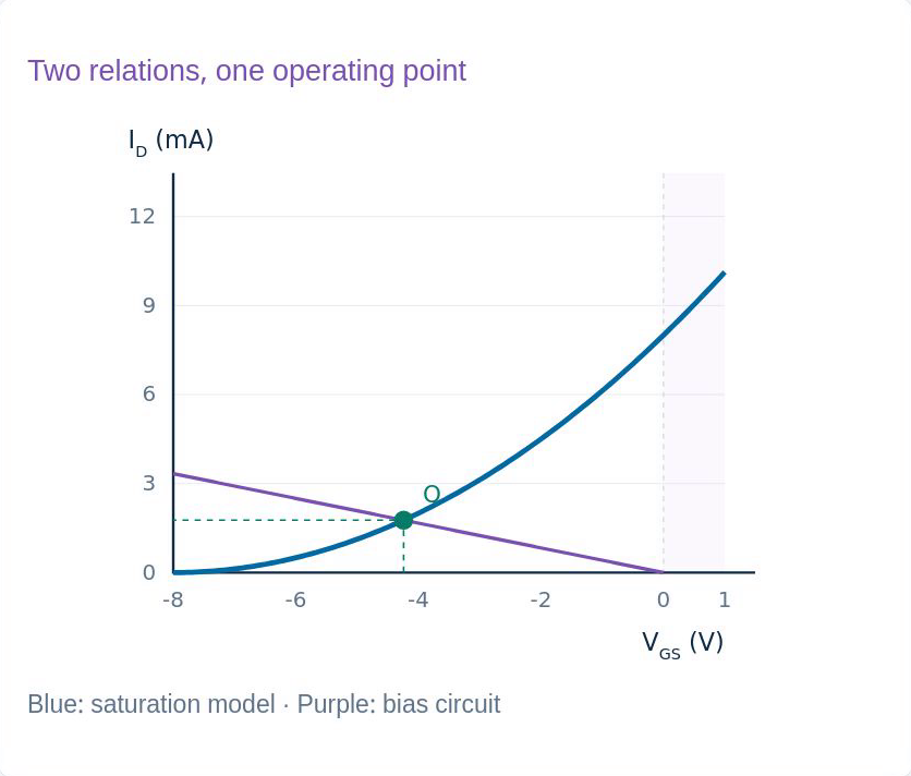
Original lesson graph; ideal DC model. Unrounded resistor + channel drops sum to 20 VDisplayed sum 19.999 V: roundingSubstitution returns the same IDNarration transcript
Now verify the complete voltage loop. The drain-resistor drop, transistor voltage, and source-resistor drop add to the twenty-volt supply when unrounded values are used. The displayed three-decimal values add to nineteen point nine nine nine volts, again just rounding. Substitute the unrounded V G S into the device equation and it returns the same drain current. These two checks confirm that the circuit and the transistor model agree, rather than merely confirming that a calculator can solve a quadratic.
14. A self-consistent operating point, not a guessed current
Self-bias line ID=−VGS/RS meets device curveQ: ID≈1.767 [mA]; VGS≈−4.240 V; region checkedAnswer: VG=0 does not mean VGS=0Narration transcript
On the graph, the purple line is the self-bias circuit relation, current equals negative gate-source voltage divided by source resistance. The blue curve is the device's saturation transfer characteristic. Their intersection gives approximately one point seven six seven milliamps and negative four point two four zero volts. The separate drain-source calculation then verified the region assumption. The gate being at zero volts did not make V G S zero: the source resistor supplied the missing part of the voltage reference.
15. A self-consistent operating point, not a guessed current
Read connections and voltage references firstTest every root and verify saturationPositive VGS is possible in general, not in this grounded-gate self-bias exampleNarration transcript
Keep four habits. Read where each resistor is connected before applying a formula. Distinguish gate-to-ground voltage from gate-source voltage. Check every algebraic root against the actual model domain, even if its current looks reasonable. Finally, compute the transistor voltage and verify saturation. A depletion MOSFET permits positive gate-source voltage in general, but this particular grounded-gate circuit produces negative self-bias. The accepted result comes from the circuit connections and the device law agreeing at one operating point.
Source video: Electronics Basics #27 | Depletion MOSFET Self-Bias: Full DC Analysis (9:30)