Electronics 1 · Electronics Basics
#32 BJT emitter–JFET drain connection: use β+1 and preserve precision
Question
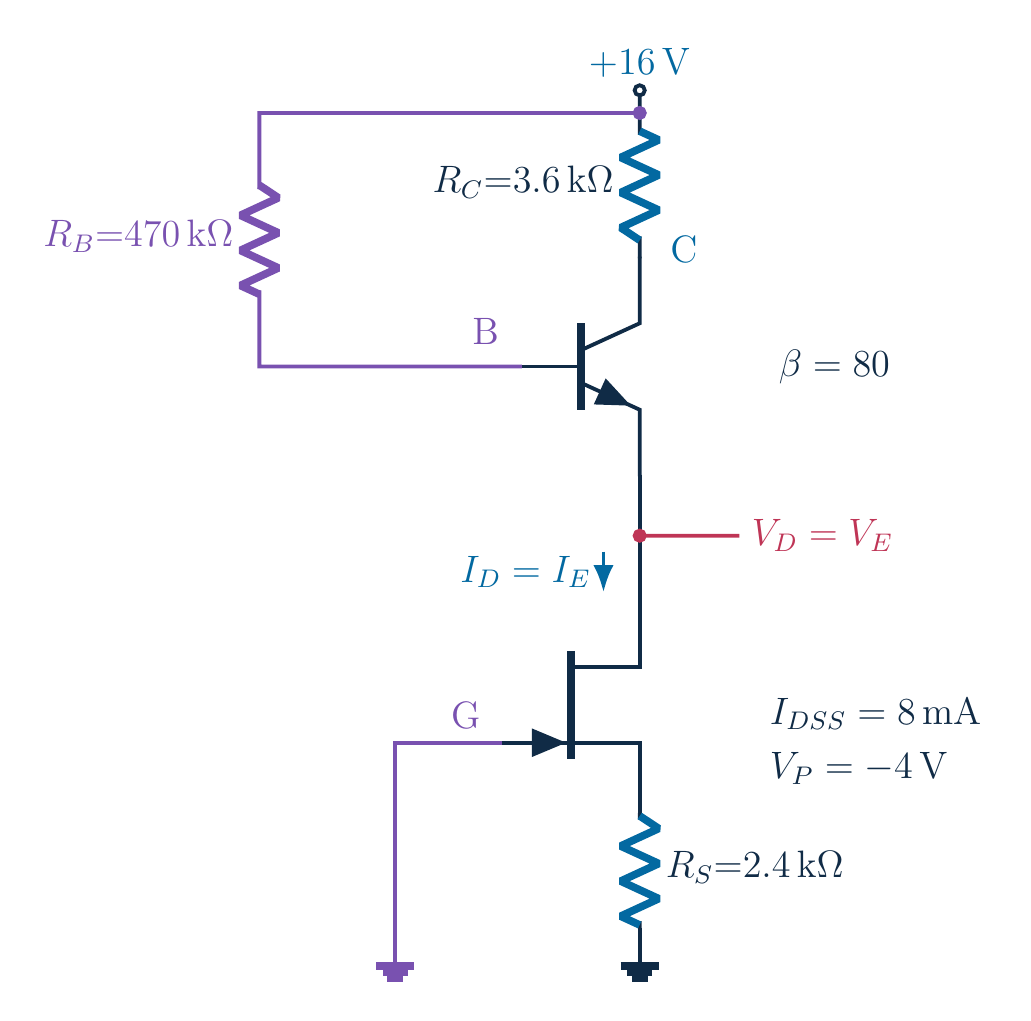
Find the red JFET drain node voltage relative to ground. This node is the BJT emitter. Use 16 V, R_C=3.6 kΩ, R_B=470 kΩ, R_S=2.4 kΩ, β=80, V_BE=0.7 V, I_DSS=8 mA and V_P=−4 V. Why divide the shared current by 81, not 80?
Written solution and narration transcript(shows the full solution)
Below are all the lines written in the notebook together with the full narration transcript.
1. Locate the requested drain voltage
Target VD to ground; JFET drain = BJT emitterGrounded gate; lower transistor sets current, upper base loop gives voltageNarration transcript
Look at the whole circuit and the red drain node. That is the voltage we want, measured relative to ground. The BJT sits above the JFET, so this time the JFET drain is also the BJT emitter. The gate is connected directly to ground. We will first find the current using the lower transistor, then use the upper transistor and its base resistor to recover the requested voltage.
2. Locate the requested drain voltage
ID=IE=(β+1)IB, not ICNarration transcript
Keep the original values: sixteen volts, a three point six kilohm collector resistor, a four hundred and seventy kilohm base resistor, and a two point four kilohm source resistor. BJT current gain is eighty. Its emitter current enters the JFET drain. Therefore drain current equals emitter current, not collector current. The emitter current includes base current, so it equals beta plus one times base current.
3. Let the grounded gate set the relation
Narration transcript
Because the gate is grounded, gate to source voltage is zero minus source voltage. The source resistor carries the JFET current. Its voltage is drain current times two point four kilohms. Combining those facts gives a negative gate to source voltage that becomes more negative as current increases. Define x as the drain current measured in milliamps; then gate to source voltage is negative two point four times x, in volts.
4. Let the grounded gate set the relation
IDSS=8 [mA]; VP=−4 V; saturation square lawx=8(1−0.6x)2; preserve outer minusNarration transcript
The JFET data are eight milliamps at zero gate bias and a cutoff voltage of negative four volts. In the assumed saturation region, use Shockley’s square law. Substituting negative two point four x for gate to source voltage leaves one minus zero point six x inside the bracket. Notice the two negative signs in the voltage ratio. Their cancellation does not turn the outer subtraction into addition.
5. Solve the current and choose the physical root
(1−0.6x)2=1−1.2x+0.36x2; multiply by 8, move xNarration transcript
Expand the square carefully. One minus zero point six x, squared, gives one minus one point two x plus zero point three six x squared. Multiply every term by eight. Then move the x from the left side to the right. The resulting quadratic is two point eight eight x squared, minus ten point six x, plus eight, equal to zero. Losing the cross term would give a different, incorrect current.
6. Solve the current and choose the physical root
Candidates: ID≈1.060 [mA] and 2.621 [mA]Test each VGS against the physical JFET intervalNarration transcript
Apply the quadratic formula. The discriminant is twenty point two. Taking both signs of its square root gives two candidates: one point zero six zero milliamps and two point six two one milliamps. Keep both for now. We do not choose a root merely because it is smaller or because it looks convenient. Each candidate must produce a gate to source voltage inside the physical JFET interval.
7. Solve the current and choose the physical root
Large root → VGS≈−6.289 VBelow −4 V cutoff: reject algebraic continuationNarration transcript
Test the larger current with the source resistor relation. It produces a gate to source voltage of about negative six point two eight nine volts. Reject this candidate. That voltage is below the negative four volt cutoff boundary. Squaring an expression below cutoff can give a positive number, but it cannot bring the ideal conducting channel back. The algebraic continuation is not a physical solution of our transistor model.
8. Solve the current and choose the physical root
Small root: VGS≈−2.544 V within [−4 V,0]VS≈+2.544 V; still need VD to check saturationNarration transcript
The smaller current gives a gate to source voltage of negative two point five four four volts. This lies between negative four volts and zero, so it is the physical candidate. Its source voltage is the opposite sign, positive two point five four four volts, because the gate is grounded. We now know the current and source voltage, but still need the drain voltage to check the saturation assumption.
9. Use the emitter current to find the drain node
IB≈13.086 [μA]; not ID/80; retain precisionNarration transcript
Use the shared current identity now. Drain current is emitter current, which equals eighty one times base current. Divide the unrounded drain current by eighty one. The base current is thirteen point zero eight six microamps. Do not divide by eighty: that would treat the known current as collector current. Do not round to thirteen microamps yet, because the large base resistor will magnify that small rounding change.
10. Use the emitter current to find the drain node
VD≈9.149 V to ground; not VDSNarration transcript
Follow the base loop from the sixteen volt supply. Subtract base current times four hundred and seventy kilohms to reach the base. Subtract the assumed zero point seven volt base to emitter drop to reach the shared emitter and drain node. Using the unrounded current, the requested drain voltage is nine point one four nine volts. This is a node voltage to ground, not the JFET drain to source voltage.
11. Verify the regions and keep enough precision
RC matters for BJT forward-active feasibilityVC≈12.231 V > VB; collector-base junction reverse biasedNarration transcript
The collector resistor did not appear in the base-loop calculation, but it is not irrelevant. It determines whether the BJT can support the assumed current in its forward active region. Collector current is eighty times base current, about one point zero four seven milliamps. Subtract its resistor drop from sixteen volts. The collector voltage is twelve point two three one volts, above the base voltage. That supports the assumed reverse biased collector to base junction.
12. Verify the regions and keep enough precision
JFET voltage:Required boundary:6.605 V > 1.456 V; both device-region checks passNarration transcript
Check the JFET separately. Drain to source voltage is the drain node minus the source node, about six point six zero five volts. The saturation boundary is gate to source voltage minus pinch off voltage, about one point four five six volts. The available voltage is larger, so saturation is consistent. Together with the BJT check, this confirms a self-consistent operating point within our stated ideal device models.
13. Verify the regions and keep enough precision
Original lesson graph; ideal model. 13.086 [μA] → about 9.15 V; 13 [μA] → 9.19 VSmall ΔIB through 470 kΩ causes about 41 [mV] differenceNarration transcript
Why do the original source versions show slightly different final numbers? One retains about thirteen point zero eight six microamps and reports nine point one five volts. The shorter version rounds base current to thirteen microamps and obtains nine point one nine volts. These describe the same circuit. A difference of only about zero point zero eight six microamps creates roughly forty one millivolts across four hundred and seventy kilohms. Keep guard digits until the final answer.
14. Read the operating point from both models
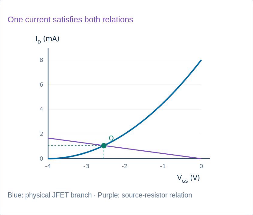
Original lesson graph; ideal model. JFET curve and self-bias line set physical ID and VGSShared emitter current → IB → VD; then check both devicesNarration transcript
The transfer graph connects the lower circuit to the device. The blue curve is the JFET law only in its physical gate voltage interval. The purple line is the source resistor relation. Their intersection gives the valid current and gate to source voltage. We then used that emitter current to calculate base current and the drain node. The graph identifies a candidate; the voltage checks establish that both transistors can operate as assumed.
15. Read the operating point from both models
Read shared terminals, reject invalid roots, keep guard digitsIdeal gate, fixed VBE and simplified laws; educational DC modelNarration transcript
Keep three habits from this example. Read which terminals share a node before equating currents. Reject roots outside the device model instead of trusting algebra alone. And preserve enough precision when a small current flows through a large resistor. We assumed negligible gate current, a fixed base to emitter drop, and ideal saturation laws. The result is a checked educational DC model, not an exact prediction for every physical device.
Source video: Electronics Basics #32 | BJT + JFET Bias: Follow the Emitter Current (7:55)