Electronics 1 · Electronics Basics
#34 Emitter degeneration: less gain, easier input drive
Question

Why deliberately reduce voltage gain? Compare two separately biased common-emitter stages with the same collector bias current: grounded emitter versus an unbypassed 200 Ω emitter resistor. Derive the input resistance and gain, keeping β+1. Numerical values are a supplementary teaching example.
Written solution and narration transcript(shows the full solution)
Below are all the lines written in the notebook together with the full narration transcript.
1. Start with the gain-versus-input tradeoff
Original same-language source. Animated panels replay the original forward segment independently of audio; matching gauges share a scale. Separate DC bias is assumed. Tradeoff: smaller output swing and less input current; both outputs invertSymbolic model; same ICQ established separately, not by adding RE aloneShared scale within each gauge family; derive and replayNarration transcript
Why would you deliberately make an amplifier produce less output? Watch two separately biased common emitter stages receive the same small input. The left emitter is at signal ground; the right has an external resistor with no bypass capacitor. Both collector outputs invert. But the right stage has a smaller output swing and takes less current from its input. That is our question: what do we gain by accepting less voltage gain? These are instruments showing a calculated signal model, not moving charges inside a transistor. Both stages have the same collector bias current, established separately. Adding a resistor alone would not preserve that operating point. Input instruments share a scale, both output instruments share a different scale, and the two base-current instruments share a third. We will derive the tradeoff and replay this experiment at the end.
2. Start with the gain-versus-input tradeoff
Original same-language source. Animated panels replay the original forward segment independently of audio; matching gauges share a scale. Separate DC bias is assumed. Input at base, output at collector; external RE has no bypassBias network omitted; separately establish forward-active QNarration transcript
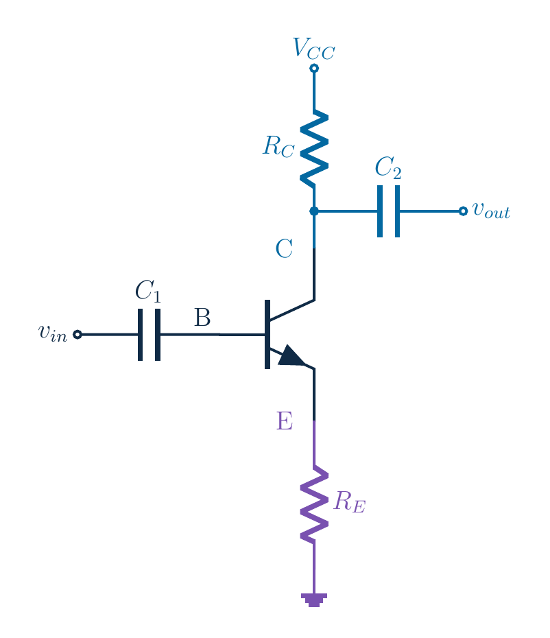
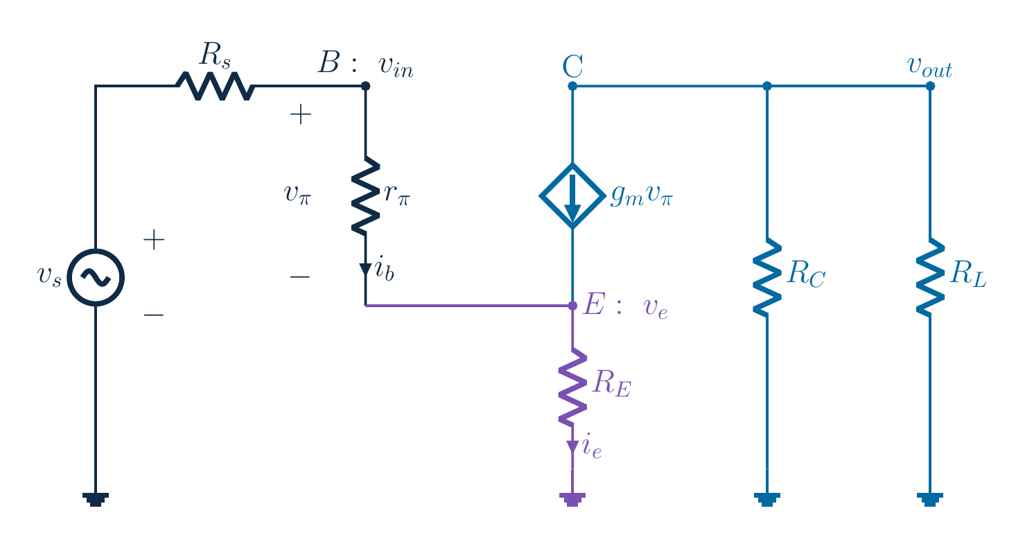
Read the actual signal path. The input reaches the base through the first coupling capacitor. The collector resistor connects to the supply, and the second capacitor takes the output from the collector. The emitter now reaches ground through an external resistor. There is no bypass capacitor across it in this lesson. The original drawing omits the base bias network. As before, assume a valid forward active operating point has already been established; this signal diagram alone is not a complete buildable amplifier.
3. The emitter is no longer signal ground
Original same-language source. Animated panels replay the original forward segment independently of audio; matching gauges share a scale. Separate DC bias is assumed. Midband: coupling capacitors ≈ shorts; supply is signal groundThis lesson takes ro → ∞, unlike the prior exampleEmitter node can move across the unbypassed RENarration transcript
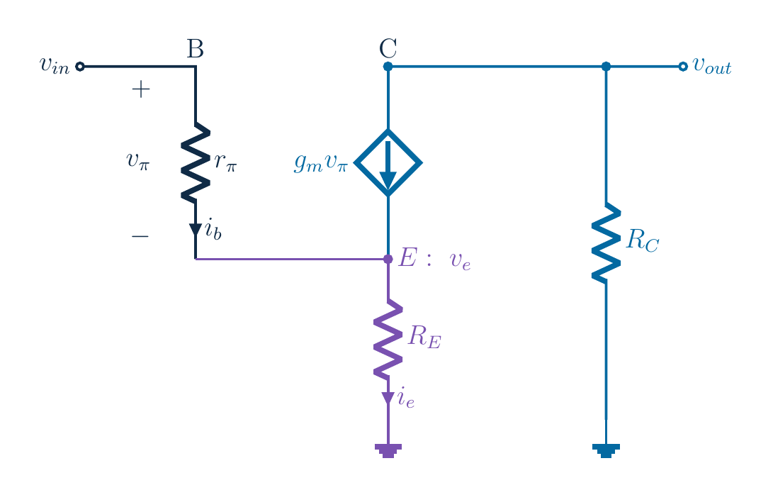
We again use a midband small signal model. Coupling capacitors are approximated as signal short circuits, transistor capacitances are neglected, and the constant supply becomes signal ground because its small signal change is zero. In this particular source, transistor output resistance is omitted: we explicitly take r o as infinite. Do not carry the finite r o from the previous numerical example into this simplified circuit. The external emitter resistor remains, so its upper node can move with the signal.
4. The emitter is no longer signal ground
Original same-language source. Animated panels replay the original forward segment independently of audio; matching gauges share a scale. Separate DC bias is assumed. Transistor responds to base–emitter gap, not base height alonevπ=vin−ve; local negative feedbackvin=ve+vπ simultaneously, not a delayed sequenceCollector still inverts; feedback reduces junction changeNarration transcript

Think of the emitter as a floor that can rise under the base. The transistor responds to the gap between them, not to the base height alone. A positive base signal raises emitter current and the voltage across the emitter resistor. Subtract that emitter voltage from the base input to obtain the controlling junction voltage. This is local negative feedback, often called emitter degeneration. In the close-up, input equals emitter voltage plus junction voltage at every instant. We are explaining the relations in order, not claiming that the circuit waits between steps: all the displayed values solve the same instantaneous model. The output is still taken at the collector and still inverts. Feedback reduces the junction change; it does not erase the input.
5. Follow both currents through the emitter resistor
RE carries ie=ib+ic, not ib aloneNarration transcript
Now identify the currents in the hybrid pi model. Base current flows through r pi from base to emitter. The controlled source adds collector current into the emitter node. Therefore the external emitter resistor carries their sum, not base current alone. Inside this model collector current is beta times base current, so emitter current is beta plus one times base current. Keeping that plus one is important when distinguishing an exact relation in the chosen model from a high beta approximation.
6. Follow both currents through the emitter resistor
Rin=rπ+(β+1)RE; before bias-network shuntingNarration transcript
Walk from the base to ground. The input voltage equals the drop across r pi plus the drop across the external emitter resistor. The first drop is base current times r pi. The second is beta plus one times base current times emitter resistance. Factor out base current and divide input voltage by it. The input resistance is r pi plus beta plus one times emitter resistance. This is the resistance looking into the transistor base in the stated model, before adding any actual base bias network in parallel.
7. Keep the minus sign and the assumptions
vo=−ic RC; more current lowers collector voltageAv=−βRC/(rπ+(β+1)RE); finite β keptNarration transcript
At the collector, current balance gives output voltage equal to negative collector current times collector resistance. The minus sign has the same origin as in the grounded emitter stage: more collector current creates more resistor drop, so collector voltage falls. Replace collector current with beta times base current and divide by the input voltage we just derived. The voltage gain is negative beta times collector resistance divided by r pi plus beta plus one times emitter resistance. No large beta approximation has been used in this step.
8. Keep the minus sign and the assumptions
Large β:Original final box missed minus sign; algebra and physics require inversionNarration transcript
There is another useful form. Since r pi equals beta divided by g m, divide the denominator by beta. Gain becomes negative g m times collector resistance divided by one plus g m times emitter resistance times one plus one over beta. The extra denominator shows the reduction caused by feedback. Only when beta is large may we neglect one over beta and write approximately negative collector resistance divided by one over g m plus emitter resistance. The final boxed formula in the original note omits a minus sign; the preceding algebra and the physics both require inversion.
9. Keep the minus sign and the assumptions
Only with large β AND g_m R_E≫1:Capital RE external; small re=VT/IEQ intrinsicgm=α/re; replacing α with 1 is an approximationNarration transcript
If g m times emitter resistance is also much greater than one, the high beta expression approaches negative collector resistance divided by emitter resistance. The gain then depends mainly on a resistor ratio, but only under both stated limits. Also keep two similarly named quantities separate. Capital R E is the external resistor. Small r e is the intrinsic emitter resistance defined as thermal voltage divided by emitter bias current. The exact identity is g m equals alpha divided by small r e. Replacing it with one over small r e is another high beta approximation.
10. Compare two stages at the same bias current
Added example:gm=0.038462 S≈38.462 mS; retain unrounded valueBias/headroom must be checked separately; supply voltage unspecifiedNarration transcript
The source gives no numbers, so these are additional teaching values. Choose one milliamp of collector bias current, beta one hundred, thermal voltage twenty six millivolts, collector resistance two kilohms, and external emitter resistance two hundred ohms. First convert units: one milliamp is zero point zero zero one amp, and twenty six millivolts is zero point zero two six volt. Transconductance is collector bias current divided by thermal voltage. Dividing zero point zero zero one by zero point zero two six gives zero point zero three eight four six two siemens, or thirty eight point four six two millisiemens. A siemens is an amp per volt. Keep the unrounded value for the next step. The bias network is assumed adjusted for forward active operation; no supply voltage is given, so actual voltage headroom still needs a separate design check.
11. Compare two stages at the same bias current
Junction resistance, not full input resistance; equal Q gives equal gm and rπNarration transcript
Next find r pi, the incremental resistance from base to emitter. Divide beta by transconductance. With the exact transconductance from the previous step, this is one hundred times zero point zero two six divided by zero point zero zero one. First multiply one hundred by zero point zero two six: that gives two point six. Then divide by zero point zero zero one: the result is two thousand six hundred ohms. Dividing by one thousand converts this to two point six kilohms. This is the junction resistance, not yet the full resistance seen at the base. Because our comparison circuits have the same separately established collector bias current and beta, they have the same r pi and transconductance.
12. Compare two stages at the same bias current
Grounded emitter: 2.6 kΩ; larger Rin means less ibNarration transcript
Now build the resistance seen at the base. We already know r pi is two thousand six hundred ohms. The emitter contribution is beta plus one times the external resistor. One hundred plus one gives one hundred one. Multiply one hundred one by two hundred ohms: that gives twenty thousand two hundred ohms. Add the junction resistance: two thousand six hundred plus twenty thousand two hundred equals twenty two thousand eight hundred ohms, or twenty two point eight kilohms. Without the external resistor, this extra term is zero and input resistance is just two point six kilohms. This larger input resistance means less base current for the same applied base voltage; it does not mean emitter current equals base current.
13. Compare two stages at the same bias current
Grounded emitter:Both negative: amplitude decreases, inversion remainsNarration transcript
Use the same input resistance to find voltage gain. The numerator is negative beta times collector resistance. Negative one hundred times two thousand gives negative two hundred thousand ohms. Divide that by twenty two thousand eight hundred ohms: gain is approximately negative eight point seven seven two volts per volt. Ohms cancel; the gain is a voltage ratio. For the grounded emitter comparison, keep the same numerator but divide by two thousand six hundred. That gives approximately negative seventy six point nine two three volts per volt. Both signs are negative, so neither circuit has stopped inverting. The resistor reduces output amplitude, not the number of inversions.
14. Compare two stages at the same bias current
Original same-language source. Animated panels replay the original forward segment independently of audio; matching gauges share a scale. Separate DC bias is assumed. ib≈4.386×10(−8) A=43.86 nAvπ=ib rπ≈0.114 [mV]; only part of the inputNarration transcript
Where does a one millivolt base signal go in the feedback stage? First calculate base current. One millivolt is zero point zero zero one volt. Divide by twenty two thousand eight hundred ohms: the result is about four point three eight six times ten to the minus eight amp. That is forty three point eight six nanoamps; nano means one billionth. Keep the unrounded current when multiplying by the two thousand six hundred ohm junction resistance. The junction voltage becomes about zero point zero zero zero one one four volt, or zero point one one four millivolt. Only a small part of the applied one millivolt reaches the controlling junction. Now we can calculate the rest instead of guessing it.
15. Compare two stages at the same bias current
Original same-language source. Animated panels replay the original forward segment independently of audio; matching gauges share a scale. Separate DC bias is assumed. Simultaneous incremental voltages, one shared scaleNarration transcript
The emitter carries beta plus one times base current. Multiply the unrounded forty three point eight six nanoamps by one hundred one: emitter current is about four point four three zero microamps. Multiplying that by two hundred ohms gives about zero point zero zero zero eight eight six volt, or zero point eight eight six millivolt at the emitter. Add the two voltage changes: zero point one one four plus zero point eight eight six equals one millivolt. That closes the input voltage loop. Finally multiply the known gain, negative eight point seven seven two, by the one millivolt input. The output change is negative eight point seven seven two millivolts. In the close-up the input, emitter and junction instruments share one scale and move simultaneously. These are changes around the bias point, not complete node voltages.
16. Compare two stages at the same bias current
Compare finite β: −8.772; 1/gm is not exactly reNarration transcript
Let us test the high beta approximation, not assume it is exact. One over transconductance is thermal voltage divided by collector current. Zero point zero two six divided by zero point zero zero one gives twenty six ohms. Add the external two hundred ohms: twenty six plus two hundred equals two hundred twenty six ohms. Divide negative two thousand by two hundred twenty six. The approximate gain is negative eight point eight five zero. Compare this with the finite beta value of negative eight point seven seven two. They are close, but the approximation is not an identity. Also, one over transconductance is not exactly the intrinsic emitter resistance: that uses emitter bias current rather than collector bias current.
17. Compare two stages at the same bias current
Resistor-ratio approximation:gm RE≈7.692; dropping 1 is still noticeableLarge β and strong feedback are distinct limits; retain full model for precisionNarration transcript
Can we simplify even further to a resistor ratio? Divide negative two thousand ohms by two hundred ohms: the result is negative ten. Why is that farther from the full model? This approximation also drops the one in the feedback denominator. With our values, transconductance times emitter resistance is zero point zero three eight four six two times two hundred, approximately seven point six nine two. That exceeds one, but is not overwhelmingly greater. Dropping the one is therefore a noticeable change. A large beta justifies one approximation; strong feedback justifies another. Do not use the second merely because the first worked. Keep the full finite beta expression when precision matters.
18. Include the source, load and model limits
Original same-language source. Animated panels replay the original forward segment independently of audio; matching gauges share a scale. Separate DC bias is assumed. With r_o → ∞ and zero input:Finite ro changes this model result and gainNarration transcript
What resistance does a load see looking back into the collector? Set the input signal to zero and remove the external load. With infinite r o, this model has no path for collector voltage to feed back into the base or emitter, so the dependent current change is zero and output resistance is simply collector resistance. This conclusion is specific to the model. Restoring finite r o changes the output resistance and gain. Emitter degeneration does not make every real transistor amplifier's output resistance exactly equal to its collector resistor.
19. Include the source, load and model limits
Separate extension:RC ∥ RL≈1666.667 Ω; unloaded Rout remains RCNarration transcript
Now change the experiment explicitly: add a ten kilohm collector load and a one kilohm source resistance. These were absent from the paired comparison. We first combine the collector resistor and the load in parallel. In ohms, their product is two thousand times ten thousand, which equals twenty million. Their sum is two thousand plus ten thousand, which equals twelve thousand. Divide the product by the sum: twenty million divided by twelve thousand is about one thousand six hundred sixty six point six six seven ohms. That is smaller than either resistor, as a parallel combination must be. Use this combined resistance for loaded gain; it does not change the definition of unloaded output resistance.
20. Include the source, load and model limits
Loaded stage gain=−β(RC ∥ RL)/RinReference is base voltage, not source voltageNarration transcript
First measure gain from the actual base input, after source resistance. The loaded stage gain is negative beta times the parallel collector resistance divided by transistor input resistance. Multiplying negative one hundred by the unrounded parallel resistance gives about negative one hundred sixty six thousand six hundred sixty six point six six seven ohms. Divide by twenty two thousand eight hundred ohms. Stage gain is approximately negative seven point three one zero. The magnitude is smaller than the unloaded eight point seven seven two because the collector load gives more current a path to signal ground. Source resistance has not yet been counted in this ratio: its denominator is the voltage at the base, not the generator voltage.
21. Include the source, load and model limits
Original same-language source. Animated panels replay the original forward segment independently of audio; matching gauges share a scale. Separate DC bias is assumed. Divider=22800/(22800+1000)Source gain≈−7.003 V/VMagnitude falls; include real bias shunt and name both gain voltagesNarration transcript
Finally include the source divider. Its denominator is twenty two thousand eight hundred plus one thousand, which equals twenty three thousand eight hundred ohms. Divide twenty two thousand eight hundred by that sum. The base receives about zero point nine five seven nine eight three of the source voltage. Multiply the unrounded loaded stage gain by this fraction. Gain measured from the source is approximately negative seven point zero zero three. Its magnitude must be smaller than the stage gain because this passive divider only reduces the input. If a real base bias network is present, include its signal resistance in parallel at the input and recalculate. Always name the two voltages in a gain ratio; source gain and stage gain are not interchangeable.
22. Include the source, load and model limits
Original unloaded comparison at 1 [mV] input: −76.923 versus −8.772 [mV] outputBoth invert; vπ≈0.114 [mV]; Rin grows 2.6 → 22.8 kΩAnswer: easier input drive and reduced gm sensitivity, a deliberate tradeoffGauge-family scales differ; check real bias, swing and frequencyNarration transcript
Return to the opening question and replay the original two-stage experiment, without the added source resistance or load. The same one millivolt input now makes the difference visible. In the grounded emitter stage the output peak change is about negative seventy six point nine two three millivolts. With the external two hundred ohm resistor, it is about negative eight point seven seven two millivolts. Both still invert. The emitter now follows most of the input, leaving only about zero point one one four millivolt across the controlling junction. The base-current instrument also moves less because input resistance rose from two point six to twenty two point eight kilohms. So why accept less gain? To make the input easier to drive and make the gain less sensitive to transistor transconductance, under our stated feedback model. This is a deliberate tradeoff, not a broken amplifier. The replay uses shared scales within each instrument family, not identical scales for every quantity. Check real bias, headroom and frequency limits before applying this signal model to hardware.
Source video: Electronics Basics #34 | Emitter Degeneration: Why Choose Less Gain? (18:47)