Electronics 1 · Electronics Basics
#36 Three input paths and finite transistor output resistance
Question

Identify every path to signal ground at the base and at the collector. How much current does the source supply, and how do finite r_o and source resistance change voltage gain? Keep the input and output ports separate.
Written solution and narration transcript(shows the full solution)
Below are all the lines written in the notebook together with the full narration transcript.
1. What loads your signal?
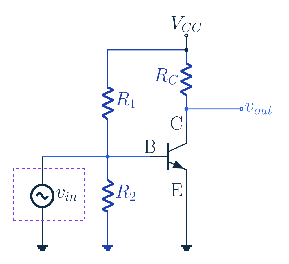
Original source. Base and collector rails are distinct nodes. Any motion panel loops forward independently of narration; symbolic gauges are not electron motion. Two questions: input loading at base and output response at collectorThree input paths; another collector path from transistor roNarration transcript
You connect a small signal to an amplifier. How much current must your source supply, and how large will the output be? Follow two separate views: look into the base to find the input resistance, then look into the collector to find the output resistance. Here the input node has three paths to signal ground. At the collector, the transistor itself adds another path. Think of parallel exits from a junction: adding an exit makes current flow easier. We will locate the exits before combining any resistors.
2. Separate DC bias from the AC model
Original source. Base and collector rails are distinct nodes. Any motion panel loops forward independently of narration; symbolic gauges are not electron motion. R1: supply→base; R2: base→ground; emitter grounded, no REEstablished forward-active Q; practical AC input must preserve DC biasNarration transcript
The original circuit uses two bias resistors. R one runs from the positive supply to the base, and R two runs from the base to ground. The collector connects through R C to the supply. The emitter is grounded: this source drawing has no emitter resistor and no drawn bypass capacitor. We analyze small changes around an already established forward active bias point. The input source symbol represents the signal, not a zero volt DC clamp that would destroy the bias. A practical zero-mean source needs suitable DC isolation.
3. Separate DC bias from the AC model
Constant supply → signal ground; both divider resistors end thereHybrid-π includes rπ, controlled current and ro; transistor ro ≠ port RoutNarration transcript
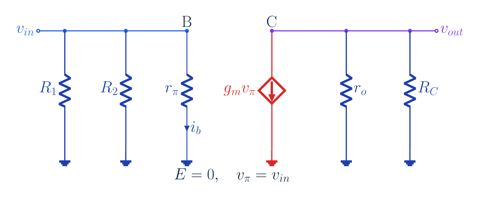
For a constant supply, the small signal change is zero. That makes the supply node signal ground in the AC equivalent; it does not mean physically shorting the power supply. R one and R two now both connect the base to signal ground. The hybrid pi model adds r pi between base and emitter, a controlled collector current, and a finite lowercase r o between collector and emitter. Lowercase r o belongs to the transistor model. Capital R out describes the resistance seen at the complete output port. They are not automatically equal.
4. One input node, three paths
Original source. Base and collector rails are distinct nodes. Any motion panel loops forward independently of narration; symbolic gauges are not electron motion. Shared two nodes, not drawing position: R1, R2 and rπ are parallel1/Rin=1/R1+1/R2+1/rπ; below smallest positive branchNarration transcript
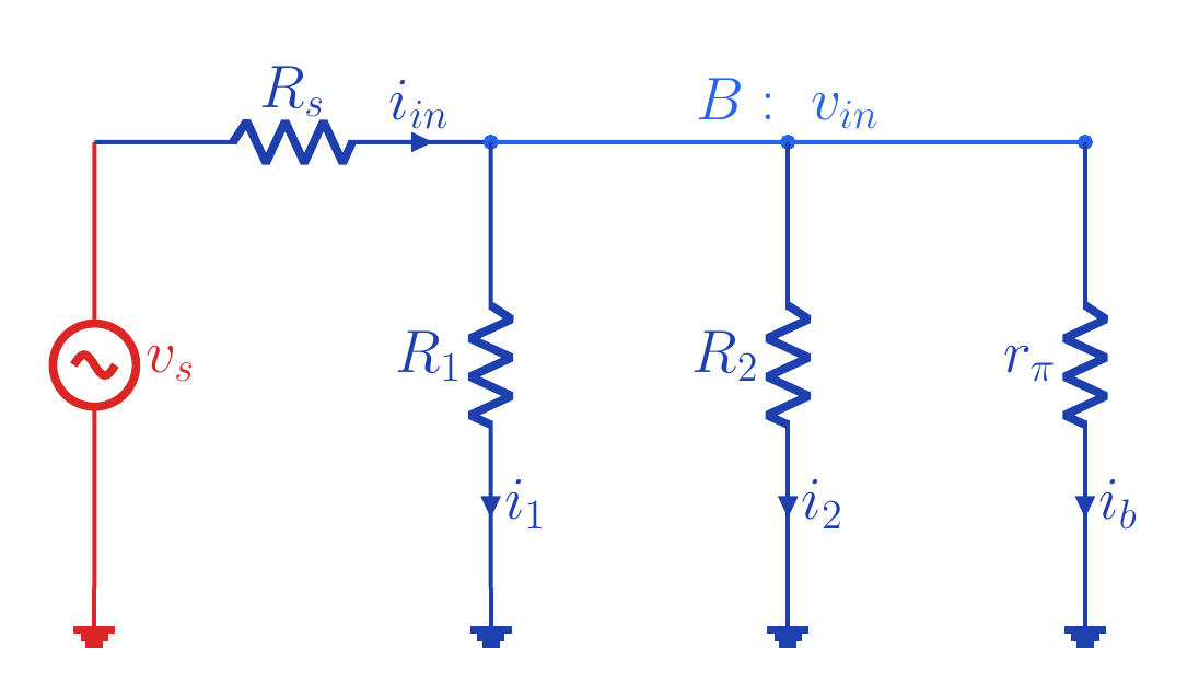
Look at the base node. Does R one become a series resistor just because it was drawn above R two? No. In the AC model, both remote ends are signal ground. R one, R two and r pi therefore share the same two nodes. All three are in parallel. The total input resistance is their parallel combination. It must be smaller than the smallest of the three finite positive resistances. That gives you a quick test before doing arithmetic.
5. One input node, three paths
Original source. Base and collector rails are distinct nodes. Any motion panel loops forward independently of narration; symbolic gauges are not electron motion. Controlled collector current=βib, not βiinGrounded emitter: vπ=vin; no emitter drop to subtractNarration transcript
Now follow the incoming current. One part flows through R one, another through R two, and only the third enters the transistor base. Kirchhoff's current law says the input current is the sum of these three branch currents. To obtain controlled collector current, multiply base current by beta, not total source current. Because the emitter is at signal ground, the voltage across r pi equals the input voltage. There is no emitter-resistor voltage to subtract in this topology.
6. Follow the collector current
Original source. Base and collector rails are distinct nodes. Any motion panel loops forward independently of narration; symbolic gauges are not electron motion. Positive base change → controlled current ↑ → collector voltage ↓Astage=−gm(RC ∥ ro); minus sign follows KCLNarration transcript
At the collector, R C and lowercase r o both lead to signal ground. A positive base voltage increases the controlled current flowing downward from collector to emitter. The collector voltage must fall so the resistor branches can supply that current. Writing all collector currents as leaving the node gives output voltage over R C, plus output voltage over r o, plus g m times input voltage, equal to zero. Solve for output voltage: the gain is negative g m times the parallel combination of R C and r o. The minus sign follows from current balance, not a memorized decoration.
7. Follow the collector current
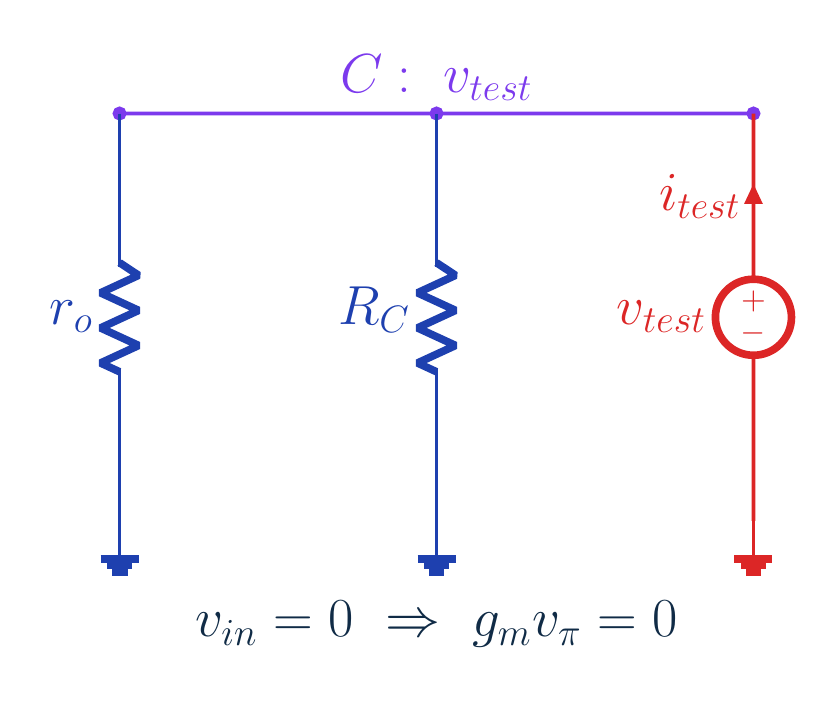
Original source. Base and collector rails are distinct nodes. Any motion panel loops forward independently of narration; symbolic gauges are not electron motion. Remove external load; zero independent input → vπ=0Rout=RC ∥ ro, not ro alonero → ∞: Rout → RC; Astage → −gm RCNarration transcript
To measure output resistance, remove any external output load and set the independent input signal to zero. In this low frequency hybrid pi model there is no collector-to-base feedback path, so the base signal becomes zero and the controlled current becomes zero. A test source at the collector sees R C in parallel with r o. That is R out, not r o alone. As r o grows without bound, R out approaches R C and the stage gain approaches negative g m R C. This limit recovers the simpler ideal model.
8. Build a numerical example
Added example:Q given; compute parameters, then input port, then output portNarration transcript
Let's use a supplemental example; these numbers are not printed in the original lesson. The established collector bias current is one milliamp, beta is one hundred, and thermal voltage is twenty five millivolts. R one is thirty kilohms, R two fifteen kilohms, R C one kilohm, and transistor output resistance fifty kilohms. We are given the operating point rather than designing its bias here. First find g m and r pi, then combine the input resistors, then combine the output resistors. Keep those two ports separate.
9. Build a numerical example
gm=1 [mA]/25 [mV]=0.04 S=40 mSNarration transcript
Transconductance, g m, tells us how much collector current changes for a small base-emitter voltage change. Divide one milliamp by twenty five millivolts. The milli factors cancel; one divided by twenty five is zero point zero four siemens, or forty millisiemens. Now divide beta, one hundred, by zero point zero four siemens. The result is two thousand five hundred ohms, or two point five kilohms. That is r pi. Its unit is resistance because dividing a dimensionless current gain by conductance gives ohms.
10. Build a numerical example
Total input 2 kΩ < 2.5 kΩ; parallel check passesNarration transcript
Combine the two divider resistors first. Thirty times fifteen is four hundred fifty, and thirty plus fifteen is forty five. Four hundred fifty divided by forty five gives ten kilohms. Now place those ten kilohms in parallel with r pi, two point five kilohms. Their product is twenty five and their sum is twelve point five. Twenty five divided by twelve point five gives two kilohms. This is total input resistance. It is smaller than two point five kilohms, just as our parallel-path check predicted.
11. Build a numerical example
Closer to 1 kΩ than 50 kΩ; larger branch does not dominateNarration transcript
At the output, combine one kilohm with fifty kilohms. The product is fifty, and the sum is fifty one. Divide fifty by fifty one: the parallel resistance is about zero point nine eight zero three nine two kilohms. Multiply by one thousand to express it as about nine hundred eighty point three nine two ohms. This is R out. Notice how close it is to one kilohm, the smaller branch, and how far it is from fifty kilohms. The larger transistor resistance does not dominate a parallel combination.
12. Build a numerical example
Original source. Base and collector rails are distinct nodes. Any motion panel loops forward independently of narration; symbolic gauges are not electron motion. Infinite ro gives −40; S×Ω dimensionless; watch milli conversionNarration transcript
We have both port resistances. Now calculate stage gain. Multiply negative zero point zero four siemens by the unrounded output resistance in ohms. The result is about negative thirty nine point two one six volts per volt. If r o were infinite, the resistance would be one thousand ohms and the gain negative forty. Finite r o has reduced the magnitude slightly, not changed the inversion. Siemens times ohms is dimensionless, which is what a voltage ratio needs. Do not multiply forty millisiemens by an ohm value as though forty were siemens.
13. Reconnect the signal source
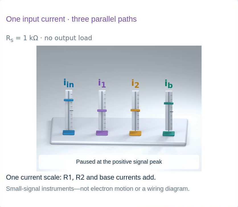
Original source. Base and collector rails are distinct nodes. Any motion panel loops forward independently of narration; symbolic gauges are not electron motion. Rs=1 kΩ; input divider=2/(1+2)=2/3Asource≈−26.144 V/V; bias resistors load source through RinNarration transcript
Now add one kilohm of source resistance. The source sees total input resistance, two kilohms. Add one and two to get three, then divide two by three. About two thirds of the source signal reaches the base. Multiply stage gain by that fraction: source to output gain is about negative twenty six point one four four. This is a different gain measurement. The two bias resistors did not disappear from the circuit just because they were absent from the stage-gain formula. They load the source through R in.
14. Reconnect the signal source
Original source. Base and collector rails are distinct nodes. Any motion panel loops forward independently of narration; symbolic gauges are not electron motion. Incremental changes; vin≪25 [mV]; full DC collector voltage need not be negativeNarration transcript
Try a one millivolt source change. Two thirds times one millivolt gives about zero point six six seven millivolts at the base. Source gain times one millivolt gives about negative twenty six point one four four millivolts at the collector. These are incremental changes around the bias point, not the full node voltages. The base change is much smaller than the twenty five millivolt thermal voltage, supporting the small signal approximation. A negative output change means the collector voltage falls a little; it does not mean the collector's DC voltage must be negative.
15. Reconnect the signal source
Answer: input R1 ∥ R2 ∥ rπ; output RC ∥ roOnly ib controls βib; source gain additionally includes input dividerShared nodes decide parallel reduction, not page positionNarration transcript
Keep one rule: identify the port, then identify every path to signal ground. At the input, R one, R two and r pi are parallel. At the output, R C and the transistor's r o are parallel. Only base current controls the beta-times-current source. Stage gain is negative g m times the output parallel resistance, while source gain also includes the input divider. The drawing may place resistors above or below each other; shared nodes, not page position, decide the reduction.
Source video: Electronics Basics #36 | Three Input Paths and Finite Transistor Output Resistance (9:54)