Electronics 1 · Electronics Basics
#37 Same DC bias, different AC gain: emitter bypass
Question

Connect a capacitor across the emitter resistor. Why can the settled DC bias stay unchanged while the AC output becomes larger? Compare emitter motion, input loading and gain, distinguishing the ideal bypass limit from a finite capacitor.
Written solution and narration transcript(shows the full solution)
Below are all the lines written in the notebook together with the full narration transcript.
1. One capacitor, a different response
Original same-language source. Independent forward-loop motion is an explanatory replay, not audio-clock synchronized. Currents share one scale; charge has a separate scale. Compare settled responses, not switch-on transients. Same settled DC bias, larger AC output: why?Track changing emitter current; power still comes from the DC supplyNarration transcript
Keep the same transistor, battery and bias resistors. Apply the same small signal, then connect a capacitor across the emitter resistor. The output can become much larger, even though the DC operating point stays the same after settling. How can both statements be true? We will compare the path taken by a steady current with the paths available to a changing current. Watch the emitter voltage as well as the output. The capacitor does not supply amplification energy; the DC power supply still does that.
2. One capacitor, a different response
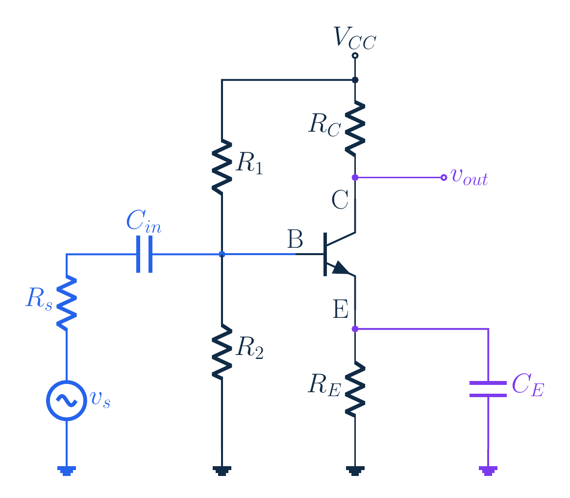
Original same-language source. Independent forward-loop motion is an explanatory replay, not audio-clock synchronized. Currents share one scale; charge has a separate scale. Compare settled responses, not switch-on transients. Steady DC: ideal capacitor open; RE still carries IEQInput coupling preserves bias; AC ground is not removing RE or shorting supplyNarration transcript
At steady DC, an ideal capacitor carries no current. The emitter resistor remains in the bias circuit. R one and R two establish the base bias, R C connects the collector to the supply, and R E carries the DC emitter current. A coupling capacitor at the input separates the source's DC level from that bias. When we later draw a signal-ground connection, it is an AC approximation, not an instruction to remove the physical resistor or short the battery. We assume the transistor has already reached a forward-active operating point.
3. Let the emitter move
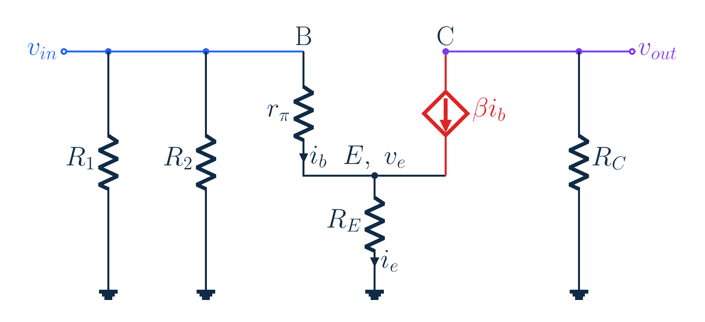
Without bypass: vin=vπ+ve; emitter movesRising emitter opposes junction change: negative feedbackHere ro → ∞; differs from previous finite-ro modelNarration transcript
First leave the bypass capacitor disconnected. In the small-signal model, the constant supply becomes signal ground. The emitter is not at signal ground, because its changing current produces a changing voltage across R E. The base voltage is the sum of the base-emitter change and the emitter change. As the base rises, the emitter rises too, opposing part of the change across the base-emitter junction. That is local negative feedback. In this lesson we take the transistor output resistance as infinite; this differs from the finite-r-o example in the previous lesson.
4. Let the emitter move
RE is not directly parallel with rπRin=R1 ∥ R2 ∥ T; divider still loads the sourceNarration transcript
Substitute both voltage changes into the input equation. The base current multiplies r pi plus beta plus one times R E. This whole expression is the transistor input branch resistance, which we call T for short. Do not place R E directly in parallel with r pi: they do not share the same two nodes. The bias resistors do each connect the base to signal ground, so total input resistance is R one, R two and T in parallel. The emitter feedback increases the transistor branch resistance, but the bias divider still loads the source.
5. Let the emitter move
Original same-language source. Independent forward-loop motion is an explanatory replay, not audio-clock synchronized. Currents share one scale; charge has a separate scale. Compare settled responses, not switch-on transients. Only large β:Narration transcript
The controlled collector current is beta times base current. Its increase lowers the collector voltage by that current times R C. Divide output voltage by input voltage; base current cancels. The exact stage gain is negative beta R C divided by T. Divide numerator and denominator by beta to obtain a denominator of one over g m plus one plus one over beta times R E. Only when beta is sufficiently large may that last factor be approximated by one. The shorter formula in the source is a high-beta approximation, not a different exact law.
6. A path for the changing current

Original same-language source. Independent forward-loop motion is an explanatory replay, not audio-clock synchronized. Currents share one scale; charge has a separate scale. Compare settled responses, not switch-on transients. Capacitor across RE: |ZC|=1/(2πfC)At suitable frequency, most changing current takes CE; ve decreasesDC feedback remains; AC feedback decreases; capacitor is not always a shortNarration transcript
Now connect the capacitor across R E. Its impedance depends on frequency: the magnitude is one divided by two pi f C. At a suitable signal frequency, its impedance is small enough that most changing emitter current takes the capacitor path. The emitter voltage then changes much less. At steady DC, the same capacitor remains an open circuit, so the resistor still establishes the emitter bias. A capacitor can therefore leave the DC feedback in place while reducing the AC feedback. It is not a short at every frequency.
7. A path for the changing current
Original same-language source. Independent forward-loop motion is an explanatory replay, not audio-clock synchronized. Currents share one scale; charge has a separate scale. Compare settled responses, not switch-on transients. Ideal bypass:Astage=−gm RC; more gain, lower input resistance; physical RE remainsNarration transcript
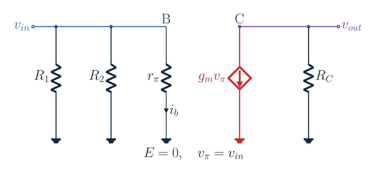
In the ideal midband bypass limit, set the emitter signal voltage to zero. Base voltage now appears across r pi. The transistor input branch becomes r pi, and total input resistance is the parallel combination of R one, R two and r pi. The stage gain becomes negative g m R C. Notice the trade-off: removing emitter AC feedback increases the gain magnitude, but decreases input resistance. The signal source must supply more current for the same base voltage. The DC resistor has not vanished from the physical circuit.
8. Compare the same operating point
Original same-language source. Independent forward-loop motion is an explanatory replay, not audio-clock synchronized. Currents share one scale; charge has a separate scale. Compare settled responses, not switch-on transients. Added example:ICQ≈1.553 [mA]; VCEQ≈7.324 V; same Q in both comparisonsNarration transcript
Use a supplemental example with a twelve volt supply. R one is eighty two kilohms, R two twenty two kilohms, R C two kilohms and R E one kilohm. Take beta as one hundred, base-emitter bias voltage as zero point seven volts, and thermal voltage as twenty six millivolts. The constant-base-emitter-voltage bias model gives a collector current of about one point five five three milliamps and a collector-emitter voltage of about seven point three two four volts. We keep that operating point in both AC comparisons. These example values are added for teaching, not copied from numerical givens in the source.
9. Compare the same operating point
gm=ICQ/26 [mV]≈59.749 mSUnbypassed T≈102.674 kΩ; branch, not total inputNarration transcript
Divide the unrounded collector bias current by twenty six millivolts. Transconductance is about fifty nine point seven four nine millisiemens. Divide beta by that conductance in siemens to obtain r pi, about one point six seven four kilohms. Without bypass, add one hundred and one times one kilohm to that r pi. The transistor input branch is about one hundred two point six seven four kilohms. This is the large branch resistance created by emitter feedback, not yet the resistance seen by the complete source.
10. Compare the same operating point
Original same-language source. Independent forward-loop motion is an explanatory replay, not audio-clock synchronized. Currents share one scale; charge has a separate scale. Compare settled responses, not switch-on transients. Astage≈−1.948; use T, not Rin, in the denominatorNarration transcript
First combine the two bias resistors: eighty two times twenty two, divided by their sum, gives about seventeen point three four six kilohms. Put that resistance in parallel with the transistor branch, using unrounded values. Total input resistance is about fourteen point eight three nine kilohms. For stage gain, negative one hundred times two kilohms divided by the transistor branch gives about negative one point nine four eight. Do not substitute total input resistance into this gain denominator: collector current is controlled by base current, not by the sum of all three input currents.
11. Compare the same operating point
Original same-language source. Independent forward-loop motion is an explanatory replay, not audio-clock synchronized. Currents share one scale; charge has a separate scale. Compare settled responses, not switch-on transients. Ideal bypass, same Q:Astage≈−119.497; high gain comes with heavier input loadingNarration transcript
Now use the ideal AC bypass limit without changing the DC bias. The transistor input branch falls from roughly one hundred two kilohms to r pi. Put the same bias-divider equivalent in parallel with r pi. Input resistance is now about one point five two six kilohms. Multiply negative g m in siemens by two thousand ohms: stage gain is about negative one hundred nineteen point four nine seven. Gain magnitude has increased dramatically, but the input has become much heavier to drive. That is why gain and input loading must be checked together.
12. Include the source and the frequency
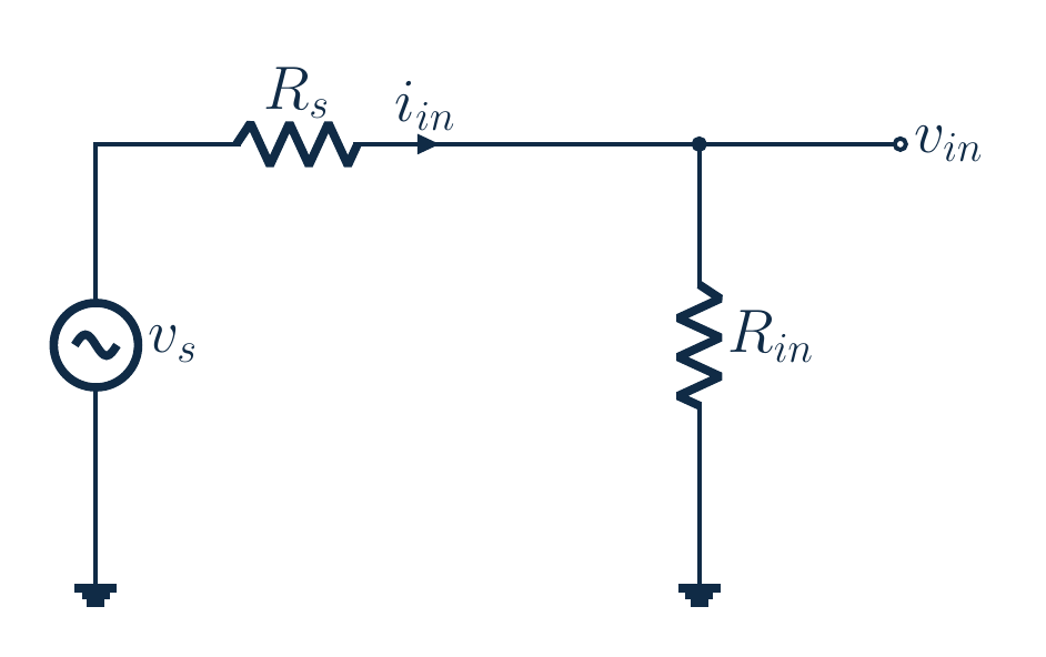
Original same-language source. Independent forward-loop motion is an explanatory replay, not audio-clock synchronized. Currents share one scale; charge has a separate scale. Compare settled responses, not switch-on transients. Rs=1 kΩ; base fraction=Rin/(Rs+Rin), changes with bypassAsource=Astage×input fraction; compare matching conditions and small vπNarration transcript
A real source has output resistance. Add one kilohm in series with our source. The fraction reaching the base is input resistance divided by source resistance plus input resistance. That fraction changes when the capacitor is connected, because input resistance changes. Source-to-output gain equals stage gain times this input fraction. Therefore, comparing two stage gains alone exaggerates the improvement for a resistive source. In either circuit, use the appropriate input resistance for that same bypass condition. Keep the input small enough for the base-emitter change to remain much smaller than thermal voltage.
13. Include the source and the frequency

Original same-language source. Independent forward-loop motion is an explanatory replay, not audio-clock synchronized. Currents share one scale; charge has a separate scale. Compare settled responses, not switch-on transients. C_E=470 μF at 1 [kHz]:Finite-capacitor |Asource|≈72.191, slight departure from 180°ie=iRE+iCE; motion, phase and values use one calculationNarration transcript
The real capacitor is finite. Use four hundred seventy microfarads at one kilohertz. Its reactance magnitude is about zero point three three nine ohms. Our full small-signal calculation keeps that impedance instead of replacing it with zero. With the one kilohm source resistance, source-gain magnitude is about seventy two point one nine one, very close to the ideal bypass limit here. It also has a small phase departure from exact inversion. The current through the capacitor and the current through R E always add to the emitter current. The animation, phase and numerical values all come from that same calculation.
14. Include the source and the frequency
Original same-language source. Independent forward-loop motion is an explanatory replay, not audio-clock synchronized. Currents share one scale; charge has a separate scale. Compare settled responses, not switch-on transients. Lower frequency → |ZC|↑ → emitter feedback returns → gain fallsCompare |ZC| to resistance seen by CE with independent sources zeroed, not just REHigh-frequency transistor capacitance and coupling-capacitor limits remainNarration transcript
Lower the signal frequency and the capacitor impedance grows. The emitter starts moving more, so its negative feedback returns and the gain falls toward the unbypassed response. The correct bypass check uses the resistance seen by the capacitor with independent signal sources set to zero; comparing its reactance only with R E is not sufficient. At the other end, real transistor capacitances eventually invalidate the midband model. We have idealized input and output coupling here to isolate the emitter capacitor. Changing those coupling capacitors would introduce additional low-frequency effects.
15. Include the source and the frequency
Answer: CE carries no steady DC but reduces changing emitter voltage and feedbackCheck settled bias, input loading and frequency-dependent gain togetherKeep RE in DC; use AC short only when justifiedNarration transcript
Return to the opening question. The DC operating point stayed the same because the ideal capacitor carries no steady current. The AC output grew because the capacitor reduced emitter motion and therefore reduced local negative feedback. In the same comparison, input resistance fell, so source loading increased. Check all three together: the settled bias point, the input loading and the frequency-dependent gain. Keep R E in the DC circuit, and replace the capacitor by an AC short only when the approximation is justified. One physical circuit can have different DC and AC equivalents without any contradiction.
Source video: Electronics Basics #37 | Emitter Bypass: Same Bias, Higher Gain? (10:45)