Electronics 1 · Electronics Basics
#38 Common-base amplifier: positive gain, low input resistance
Question

Hold the base steady and raise the emitter slightly. Does the collector rise or fall? Explain the signs, derive the input resistance and distinguish stage gain from source-to-output gain.
Written solution and narration transcript(shows the full solution)
Below are all the lines written in the notebook together with the full narration transcript.
1. Raise the emitter: what happens?
Original source figure. The forward-loop motion is an independent explanatory replay, not synchronized to the audio clock. It shows small changes around the DC operating point, not electron trajectories. Hold the base steady; raise the emitter: which way does the collector move?Same transistor, different input port; observe changes around the settled Q pointNarration transcript
The collector output in our common-emitter examples fell when the input rose. Now keep the base steady and apply a tiny signal to the emitter instead. Will the collector still move in the opposite direction? Watch the emitter, the base-emitter voltage and the collector together. The transistor is unchanged, but the input port is different. We will first predict the direction of motion, then calculate the gain and the resistance seen by the source. The moving instruments show changes around a settled operating point, not the full DC voltages.
2. Raise the emitter: what happens?
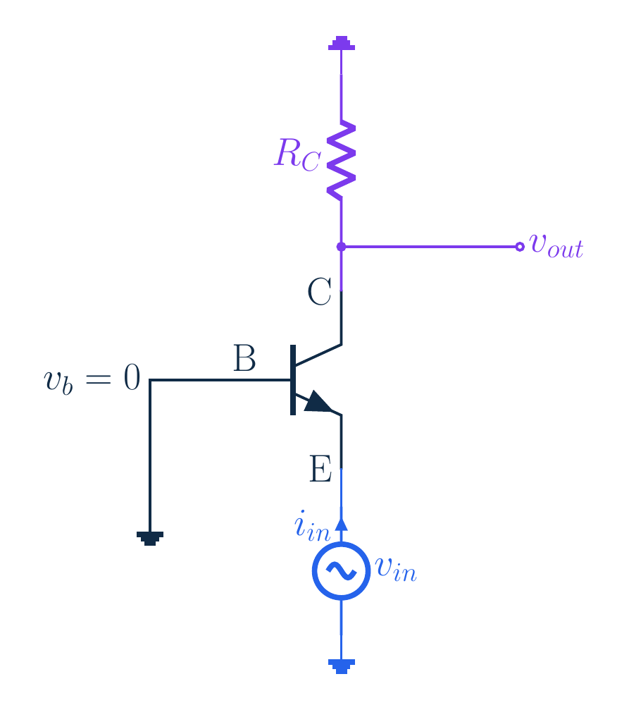
Original source figure. The forward-loop motion is an independent explanatory replay, not synchronized to the audio clock. It shows small changes around the DC operating point, not electron trajectories. AC ground at the base does not mean zero DC base voltageInput: emitter; output: collector; supply is AC groundAssume ro → ∞ and neglect internal capacitance; not a bias-design problemNarration transcript
Signal ground means that the base voltage does not change with this input. It does not mean the physical base must sit at zero volts DC. A bias arrangement establishes the operating point, while an ideal AC connection keeps the base steady. The input enters the emitter and the output is measured at the collector. R C connects the collector to the supply; the supply is also signal ground in the AC model. We ignore the transistor output resistance and internal capacitances here. Bias-network design and turn-on transients are outside this particular source lesson.
3. Choose the port and keep the signs
Emitter rises → base-emitter voltage falls; current arrows are unchangedNarration transcript
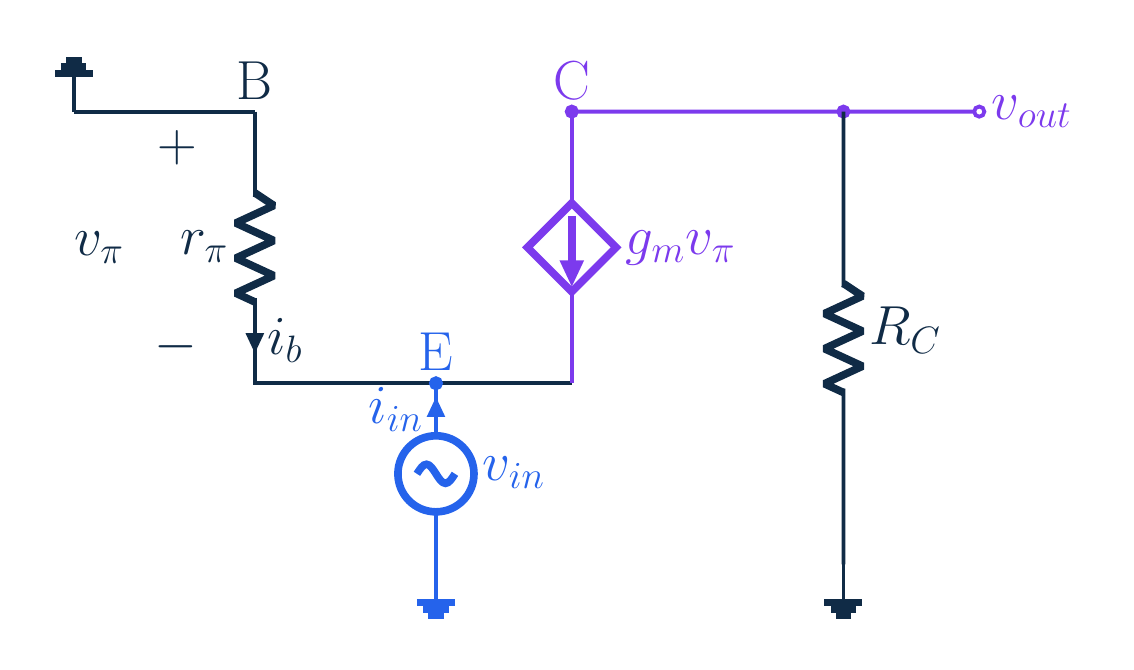
Define v pi as the voltage at the base minus the voltage at the emitter, just as before. The base signal is zero, while the emitter signal is the input. Therefore v pi is negative v in. If the emitter rises slightly, the base-emitter voltage decreases. This sign is the key to the entire lesson. We have not changed the transistor law or flipped its controlled-current arrow. We changed where the signal enters, so the same base-emitter voltage now has the opposite sign to the input.
4. Choose the port and keep the signs
ib=vπ/rπ; ic=βib; arrows B→E and C→EInput current enters E:Positive vin: ib<0, ic<0, but iin>0Narration transcript
Keep base current positive from base to emitter, and collector current positive from collector to emitter. In the hybrid-pi model, base current equals v pi divided by r pi, and collector current equals beta times base current. Define input current as positive entering the emitter port. Kirchhoff's current law gives input current as negative base current minus collector current. Substituting the collector relation gives the negative of the sum beta plus one, multiplied by base current. For a positive emitter signal, both transistor current changes are negative, but the current entering the input port is positive.
5. Derive the three stage properties
For large β only:Narration transcript
Input resistance is input voltage divided by input current. Replace the input voltage with negative v pi and the input current with the negative of the sum beta plus one, multiplied by base current. The two minus signs cancel. Since v pi divided by base current is r pi, the input resistance is r pi divided by beta plus one. Using r pi equals beta over g m, the same result is alpha over g m, where alpha is beta divided by beta plus one. For large beta this is close to one over g m, but that final step is an approximation.
6. Derive the three stage properties
Original source figure. The forward-loop motion is an independent explanatory replay, not synchronized to the audio clock. It shows small changes around the DC operating point, not electron trajectories. Emitter↑ → vπ↓ → ic↓ → drop across RC↓ → collector↑; supply provides energyNarration transcript
Now follow the output. The collector signal voltage is negative collector-current change times R C. Substitute collector current equals g m v pi, then replace v pi with negative input voltage. The minus signs cancel again. Stage voltage gain is positive g m R C. Observe the causal chain: the emitter rises, base-emitter voltage falls, collector current falls, the voltage drop across R C shrinks, and collector voltage rises. Input and output therefore rise together in this midband model. The supply still provides the energy for the amplified output.
7. Derive the three stage properties
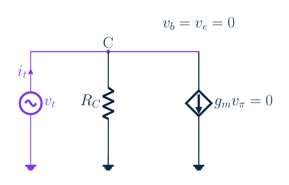
Original source figure. The forward-loop motion is an independent explanatory replay, not synchronized to the audio clock. It shows small changes around the DC operating point, not electron trajectories. Zero independent input signal: vb=ve=0, so gm vπ=0Rout=RC for infinite transistor roKeep DC bias; finite ro or real bias networks change the resultNarration transcript
To find output resistance, turn off the independent input voltage source. The emitter becomes signal ground, as does the base, so v pi is zero. The controlled current source then carries zero small-signal current. With infinite transistor output resistance, a test applied at the collector sees only R C to signal ground. Output resistance is R C. This conclusion relies on the stated model: a finite output resistance or a real bias network can change the analysis. Turning off the signal does not turn off the DC bias that defines g m.
8. A complete numerical check
VCC=12 V; VB=1.2 V; VE=0.5 V; VC=10 V>VB: forward activeNarration transcript
For a supplemental example, let the bias arrangement establish an emitter current of one point zero one milliamps with beta equal to one hundred. Collector current is then exactly one milliamp in this model. Use a thermal voltage of twenty five millivolts and R C of two kilohms. A twelve volt supply, a base bias of one point two volts and a base-emitter bias of zero point seven volts place the emitter at zero point five volts and the collector at ten volts. The collector is above the base, so this operating point is forward active.
9. A complete numerical check
Original source figure. The forward-loop motion is an independent explanatory replay, not synchronized to the audio clock. It shows small changes around the DC operating point, not electron trajectories. gm=1 [mA]/25 [mV]=0.04 S=40 mSApproximation 1/gm=25 Ω; exact relation retains β+1Narration transcript
Divide one milliamp by twenty five millivolts. Transconductance is zero point zero four siemens, or forty millisiemens. Divide beta, one hundred, by zero point zero four siemens. R pi is two thousand five hundred ohms. Next divide that resistance by one hundred and one. The emitter input resistance is about twenty four point seven five two ohms. In contrast, the approximate one over g m gives twenty five ohms. The values are close here, but retaining beta plus one makes the calculation consistent with the exact current relation.
10. A complete numerical check
Original source figure. The forward-loop motion is an independent explanatory replay, not synchronized to the audio clock. It shows small changes around the DC operating point, not electron trajectories. vo=+20 [mV]; total IC=0.99 [mA], not reversed; |vπ|≪VTNarration transcript
For stage gain, multiply zero point zero four siemens by two thousand ohms. The result is positive eighty volts per volt. Apply a positive quarter millivolt directly to the emitter with an ideal source. V pi is negative a quarter millivolt, so collector current changes by negative ten microamps. Multiplying that current change by negative two kilohms gives positive twenty millivolts at the output. The full collector current falls from one milliamp to zero point nine nine milliamps; it does not reverse. The tiny signal is also much smaller than the twenty five millivolt thermal voltage.
11. Include the source and return to the question
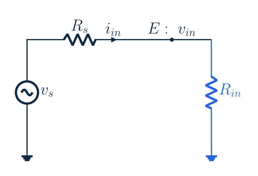
Rs=50 Ω; input fraction=Rin/(50+Rin)≈0.3311Asource=80×input fraction≈+26.49vs=0.25 [mV] → vin≈0.0828 [mV] → vo≈6.623 [mV]; identify the measurement portNarration transcript
A source with internal resistance does not deliver its full voltage to this low-resistance input. Place fifty ohms in series with the source. The input fraction is R in divided by fifty ohms plus R in, about zero point three three one one. Multiply that fraction by the stage gain of eighty. Gain measured from the source is about positive twenty six point four nine, not eighty. With the same quarter millivolt source peak, the emitter receives about zero point zero eight two eight millivolts and the output is about six point six two three millivolts. Always say where the input voltage is measured.
12. Include the source and return to the question
|ic|/iin=α=100/101≈0.9901, not voltage gain80Low input resistance permits large voltage gain; signed ic/iin=−αNarration transcript
A voltage gain of eighty does not imply a current gain of eighty. Compare the magnitude of collector-current change with the current entering the emitter input. From the same sign definitions, that ratio is beta divided by beta plus one, called alpha. With beta equal to one hundred, alpha is about zero point nine nine zero one, slightly less than one. A relatively low input resistance and a much larger collector resistance allow a large voltage change without a large current gain. The signed ratio of our downward collector-current arrow to the entering input-current arrow is negative alpha.
13. Include the source and return to the question
Original source figure. The forward-loop motion is an independent explanatory replay, not synchronized to the audio clock. It shows small changes around the DC operating point, not electron trajectories. Small-signal forward-active model; large signal, capacitance, finite ro and load change itBase AC-ground impedance must actually be low; otherwise vπ≠−vinNarration transcript
Our equations describe small changes around a forward-active bias point. If the input becomes too large, the base-emitter exponential law and cutoff or saturation invalidate the linear result. At sufficiently low or high frequencies, coupling and internal capacitances also matter. A finite transistor output resistance or an added output load changes the output equations. Finally, AC ground at the base must really be a low impedance at the frequencies of interest. A moving base would change v pi from simply negative input voltage. The clean formulas are useful because we have made these assumptions explicit.
14. Include the source and return to the question
Answer: emitter↑ → vπ↓ → ic↓ → RC drop↓ → collector↑Ideal emitter input: +80; with Rs=50 Ω source gain≈+26.49; always check port and loadingNarration transcript
Return to the opening experiment. Raise the emitter while the base stays steady. Base-emitter voltage decreases; collector current decreases; the drop across R C decreases; the collector rises. That visible chain explains the positive voltage gain of the common-base stage. In our example an ideal quarter millivolt emitter signal produces a twenty millivolt collector signal of the same sign. The stage gain is eighty, but adding fifty ohms of source resistance reduces source-to-output gain to about twenty six point four nine. Remember the port, the reference arrows and the loading before choosing a formula.
Source video: Electronics Basics #38 | Common Base: Why Is the Gain Positive? (10:04)