Electronics 1 · Electronics Basics
#39 MOSFET common source: gate control and finite output resistance
Question

The ideal gate draws no signal current. Why does a small positive gate voltage still lower the drain voltage, and why does finite transistor output resistance reduce gain?
Written solution and narration transcript(shows the full solution)
Below are all the lines written in the notebook together with the full narration transcript.
1. A voltage-controlled change
Original same-language source. Forward-loop motion is an independent explanatory replay, not synchronized to audio. Instruments show small changes around bias, not full semiconductor simulation. Raise the gate by 1 [mV]; ideal gate current is zero. Does the drain respond?Gate controls drain-current change; RD converts it to an inverted voltageNarration transcript
Imagine raising a MOSFET gate voltage by just one millivolt. In our ideal midband model, no signal current enters the gate. Does that mean nothing can happen at the drain? Watch the gate signal and the drain voltage together. The gate controls a change in drain current without receiving that current itself. The drain resistor converts the change into an output voltage. We will explain why the output falls, and why the transistor's finite output resistance makes the gain smaller than the simplest estimate.
2. A voltage-controlled change
Original same-language source. Forward-loop motion is an independent explanatory replay, not synchronized to audio. Instruments show small changes around bias, not full semiconductor simulation. Grounded source; gate input, drain output; constant supply becomes AC groundCoupling capacitors short only in the stated band; keep saturation bias separateNarration transcript
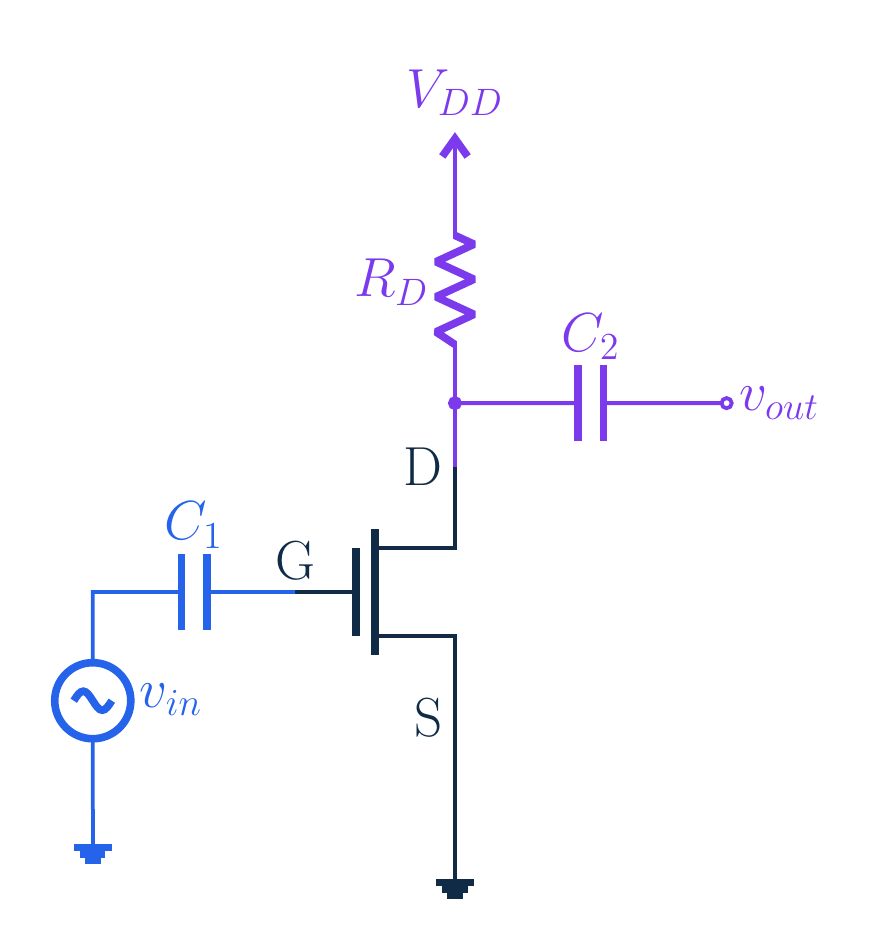
The source is grounded. The input is applied to the gate and the output is taken from the drain. R D connects the drain to the DC supply. For the small-signal circuit, a constant supply becomes AC ground. The coupling capacitors are approximated as shorts only in the frequency range we are studying. An established bias arrangement keeps the MOSFET in saturation; the simplified AC drawing does not design that arrangement. Keep the settled bias separate from the tiny changes drawn on the instruments.
3. A voltage-controlled change
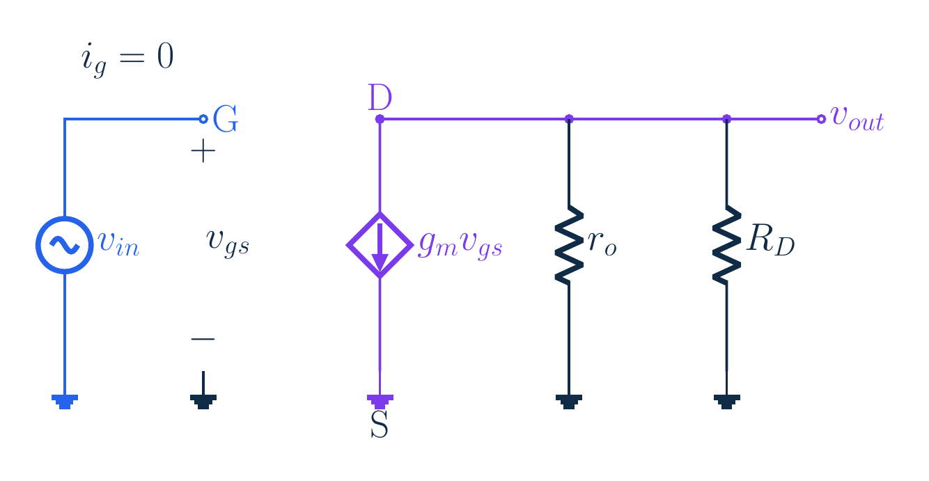
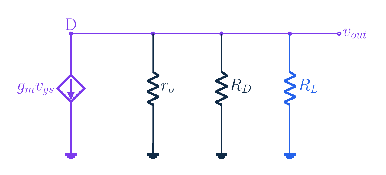
Controlled source gm vgs and ro connect drain to source; ro is a local slopeRD ∥ ro at the output; all branches obey the same current balanceNarration transcript
Replace the MOSFET by a controlled current source from drain to source, with value g m times v g s, and a resistance r o between the same two terminals. R o represents the local slope of the drain-current versus drain-voltage characteristic. It is not a resistor at the gate and not the external drain resistor. Since the source and supply are both AC ground, r o and R D appear in parallel at the output. The controlled source and both passive paths must satisfy the same current balance.
4. Find the input and output resistances
Original same-language source. Forward-loop motion is an independent explanatory replay, not synchronized to audio. Instruments show small changes around bias, not full semiconductor simulation. Ideal insulated gate, no capacitance: ig=0 → intrinsic Rin→∞Real bias resistors, capacitance and leakage limit impedance; ideal open gate has no divider lossNarration transcript
Input resistance is the input voltage divided by the input current. With an insulated ideal gate and capacitances neglected, the gate current is zero. Therefore the intrinsic input resistance is infinite. This is a model statement, not a claim that every real amplifier input has infinite impedance. Gate-bias resistors provide additional input paths, and gate capacitance draws changing current at higher frequencies. A series source resistance causes no divider loss against the ideal open gate, but it can matter once those omitted paths are included.
5. Find the input and output resistances
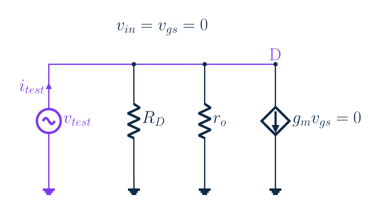
Zero input signal but retain DC bias; vgs=0; drain test sees RD ∥ roRout=RD ∥ ro; as ro→∞, Rout→RD; external load is separateNarration transcript
To find output resistance, set the independent input signal to zero while retaining the DC bias that establishes g m. Now v g s is zero, so the controlled current source becomes zero. Apply a test voltage at the drain. Its current flows through R D and r o in parallel. Therefore output resistance is R D parallel r o. Output resistance is a port property; it is not the same thing as a later external load. If r o tends to infinity, this result approaches R D.
6. Derive gain and transconductance
Grounded source: vgs=vin; Av=−gm(RD ∥ ro); gate↑ → drain↓Narration transcript
Return to the current balance at the drain. The output voltage multiplied by the sum of the two conductances must cancel g m times v g s. Solving gives output voltage equal to negative g m times v g s times R D parallel r o. The grounded source makes v g s equal to the input voltage. Divide by that input and obtain voltage gain: negative g m times R D parallel r o. The negative sign means a positive gate change produces a negative drain change around the bias point.
7. Derive gain and transconductance
Original same-language source. Forward-loop motion is an independent explanatory replay, not synchronized to audio. Instruments show small changes around bias, not full semiconductor simulation. Ideal long-channel square law: k=μCox(W/L); ID=kVOV²/2gm=kVOV=√(2kID)VGS=VTH+√(2ID/k); ideal gm estimate is not a complete finite-ro modelNarration transcript
Where can g m come from? In the ideal long-channel saturation square law, define k as mobility times oxide capacitance per area times the width-to-length ratio. Drain current is one half k times overdrive voltage squared. Differentiating with respect to gate-source voltage gives g m equal to k times overdrive. Equivalently, g m is the square root of two k I D. Rearranging the same current law gives V G S equal to threshold plus the square root of two I D divided by k. These ideal relations estimate g m; they are not a complete model of finite output resistance.
8. Check one consistent operating point
IDQ=1 [mA]; gm=2 mS; RD=4.7 kΩ; ro=50 kΩ; VD=7.3 V>VOV=1 VSupplemental values; ideal square-law illustration:Narration transcript
Use a supplemental example with drain bias current one milliamp, g m two millisiemens, R D four point seven kilohms, r o fifty kilohms and a twelve volt supply. A one volt overdrive leaves the drain at seven point three volts, comfortably above the saturation boundary in this simplified model. The original Turkish source provides no numerical values; these are teaching choices. Separately, the ideal square law with k two milliamps per volt squared and threshold one volt gives one volt overdrive, two volts gate-source bias and the same two millisiemens g m.
9. Check one consistent operating point
Original same-language source. Forward-loop motion is an independent explanatory replay, not synchronized to audio. Instruments show small changes around bias, not full semiconductor simulation. ΔiD=gm vgs+vo/ro≈1.828 [μA], not 2 [μA]Narration transcript
Calculate the parallel resistance using four thousand seven hundred times fifty thousand, divided by their sum. The result is about four thousand two hundred ninety six point one six one ohms. Multiply by negative zero point zero zero two siemens. Voltage gain is about negative eight point five nine two volts per volt. A positive one millivolt input gives negative eight point five nine two millivolts output. The controlled-source increment is positive two microamps. The r o branch has a negative current increment, so the total transistor drain-current increment is about one point eight two eight microamps, not exactly two.
10. Check one consistent operating point
Original same-language source. Forward-loop motion is an independent explanatory replay, not synchronized to audio. Instruments show small changes around bias, not full semiconductor simulation. Same gm and RD, ro→∞: Av=−9.4; vo=−9.4 [mV] for +1 [mV]Finite ro reduces resistance and gain magnitude, not inversion; compare local modelsNarration transcript
Now compare the same local g m and drain resistor while increasing r o toward infinity. The parallel resistance approaches four point seven kilohms. The idealized gain becomes negative nine point four volts per volt, and a one millivolt input produces negative nine point four millivolts. The finite resistance did not change the inversion. It reduced the effective output resistance and the magnitude of gain. We are comparing two local small-signal models with the same stated bias parameters, not physically changing a device parameter without consequences.
11. State the limits and answer the question
External AC-coupled R_L:Own Rout excludes external load; real gate-bias resistance also limits RinNarration transcript
If an external load is attached through an ideal midband coupling capacitor, it adds a third output path. Replace the two-resistance parallel combination by R D parallel r o parallel R L. The loaded voltage gain is negative g m times that combination. But the amplifier's own output resistance remains the port value found with the external load removed. At the input, an actual gate-bias resistance would similarly limit the input resistance. State what belongs to the amplifier and what has been attached to it before quoting a resistance or a gain.
12. State the limits and answer the question
Original same-language source. Forward-loop motion is an independent explanatory replay, not synchronized to audio. Instruments show small changes around bias, not full semiconductor simulation. Small signal around saturation only; large signal and frequency effects change the modelTemperature/fabrication shift Q; check headroom and state all assumptionsNarration transcript
The model is linear only for small excursions around the chosen saturation bias. Large inputs can make g m vary significantly or drive the device out of saturation. Real gates have capacitance and leakage, and coupling capacitors cannot be short circuits at every frequency. Temperature and fabrication also change the operating point. These instruments visualize a calculated local model, not a complete semiconductor simulation. The useful habit is to name the assumptions before applying a compact gain formula and to check that the predicted voltages remain inside the allowed operating region.
13. State the limits and answer the question
Answer: gate↑ → controlled drain current↑ → drain voltage↓, even with ig=0Finite ro adds an output path: −8.592 [mV] versus ideal −9.4 [mV] for +1 [mV] inputNarration transcript
Return to the opening question. Raise the gate while the source stays fixed. The controlled drain current rises, so the drain voltage falls. No signal current has to enter the ideal gate for this voltage control to occur. With finite r o, the output-current balance includes another path, reducing output resistance and gain magnitude. Our one millivolt gate change gives about negative eight point five nine two millivolts at the drain, compared with negative nine point four in the infinite r o limit. That is the mechanism behind negative g m times R D parallel r o.
Source video: Electronics Basics #39 | MOSFET Common Source: Why Does the Output Fall? (9:07)