Electronics 1 · Electronics Basics
#40 MOSFET source degeneration: sharing the input
Question

With an unbypassed source resistor, does a 1 mV gate signal still appear entirely across gate and source? Derive the voltage sharing, gain and limits of the large-feedback approximation.
Written solution and narration transcript(shows the full solution)
Below are all the lines written in the notebook together with the full narration transcript.
1. The gate rises, but so does the source
Original same-language source. Independent forward-loop explanatory motion, not audio-clock synchronization. Gate, source and gate-to-source markers share a voltage scale; retain the stated settled bias. Add an unbypassed source resistor: does the MOSFET feel all of a 1 [mV] gate input?Source rises too → smaller vgs → smaller drain swing; compare settled small signalsNarration transcript
Raise the gate of a MOSFET by one millivolt. In the previous grounded-source stage, that whole change appeared between gate and source. Now put an unbypassed resistor under the source. Does the transistor still feel the entire millivolt? Watch the gate, the source and their difference together. The source can rise too, leaving a smaller gate-to-source change and a smaller drain swing. We will derive that sharing from Kirchhoff's law, then test it with one complete example. The moving instruments represent small changes around a settled bias point, not a turn-on animation.
2. The gate rises, but so does the source
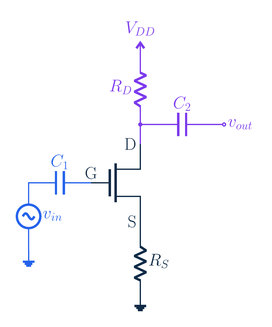
Original same-language source. Independent forward-loop explanatory motion, not audio-clock synchronization. Gate, source and gate-to-source markers share a voltage scale; retain the stated settled bias. Gate input, drain output; RS remains in AC; establish a valid saturation biasHere ro→∞ and capacitances neglected, unlike the previous finite-ro lessonNarration transcript
The input is applied to the gate and the output is taken at the drain. R D connects the drain to the supply. R S connects the source to ground and remains in the AC circuit because no bypass capacitor shorts it. A separate bias arrangement establishes a valid saturation operating point. In this source lesson we neglect the intrinsic drain-to-source output resistance and internal capacitances. That differs deliberately from the finite output resistance retained in the previous lesson. The supply is signal ground, but its DC voltage still sets the bias and available output headroom.
3. Follow the controlling voltage
Original same-language source. Independent forward-loop explanatory motion, not audio-clock synchronization. Gate, source and gate-to-source markers share a voltage scale; retain the stated settled bias. Gate↑ → current↑ → source↑ → vgs opposed: local negative feedbackNarration transcript
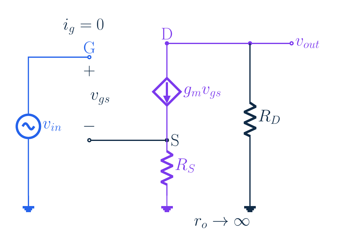
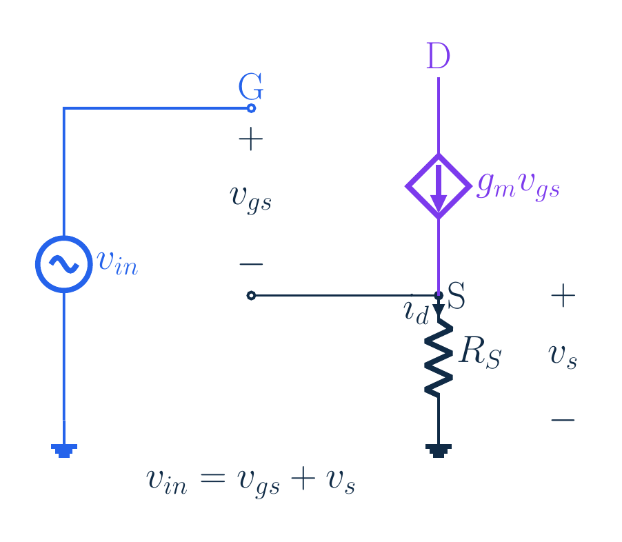
The ideal MOSFET gate draws no small-signal current in this midband model. Keep the controlled drain current positive from drain to source. It equals g m times v g s. With infinite intrinsic output resistance, the same incremental current flows through the source resistor. The source voltage is therefore g m times v g s times R S. When a positive gate change increases drain current, the source resistor raises the source voltage. That upward source motion reduces the gate-to-source voltage responsible for the original increase. This is local negative feedback, even though the source voltage moves in the same direction as the gate.
4. Follow the controlling voltage
vs=[gm RS/(1+gm RS)]vin; fractions sum to 1Narration transcript
Gate voltage relative to ground is gate-to-source voltage plus source voltage. Substitute the source-resistor relation into that sum. The input becomes v g s multiplied by one plus g m R S. Divide by that entire factor to obtain the controlling voltage. Thus v g s equals input voltage divided by one plus g m R S. The source gets the remaining part: g m R S divided by one plus g m R S, multiplied by the input. These two fractions add to one. The MOSFET law has not changed; the source motion changes how much input reaches its controlling voltage.
5. Gain and the two port resistances
Original same-language source. Independent forward-loop explanatory motion, not audio-clock synchronization. Gate, source and gate-to-source markers share a voltage scale; retain the stated settled bias. Av=−RD/(1/gm+RS); still inverting; no BJT β+1 factorNarration transcript
A positive incremental drain current increases the drop across R D, so the drain output falls. The output is negative g m R D times v g s. Now substitute the controlling-voltage fraction. The voltage gain becomes negative g m R D divided by one plus g m R S. Divide numerator and denominator by g m to write the equivalent result as negative R D divided by the sum of one over g m and R S. The output still inverts, but its magnitude is smaller than the grounded-source result at the same g m. Do not insert a BJT beta-plus-one factor into this MOSFET equation.
6. Gain and the two port resistances
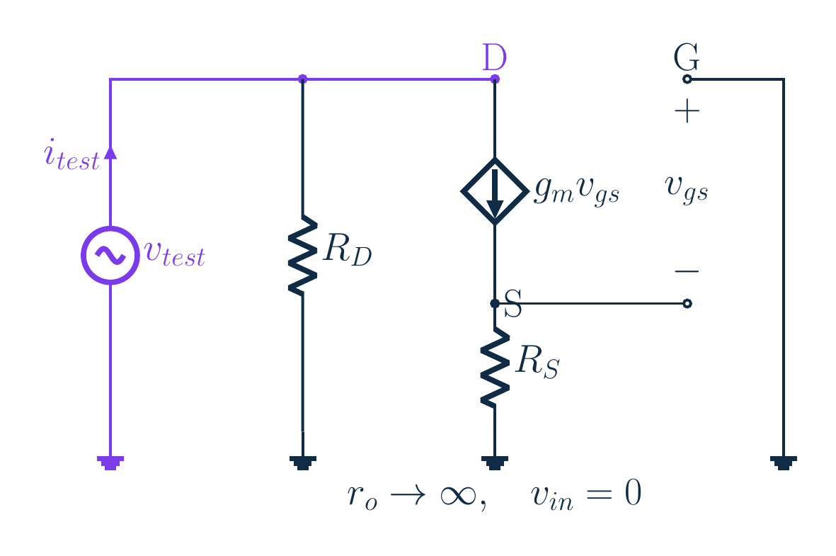
Original same-language source. Independent forward-loop explanatory motion, not audio-clock synchronization. Gate, source and gate-to-source markers share a voltage scale; retain the stated settled bias. Ideal Rin→∞ without gate-bias resistance; real bias network makes it finiteZero gate signal and ro→∞ → vs=0; output test gives Rout=RDNarration transcript
With no gate current and no gate-bias resistor included in the port, the ideal input resistance is infinite. A real gate-bias network would appear in parallel and make it finite. For output resistance, set the independent gate signal to zero and apply a test voltage at the drain. Under our infinite intrinsic output resistance assumption, the drain voltage cannot control the source node. The source-node equation gives zero source signal, so v g s and the controlled current are zero. The test source therefore sees only R D. This result depends on the model: restoring finite intrinsic output resistance changes the test circuit.
7. A numerical experiment
Original same-language source. Independent forward-loop explanatory motion, not audio-clock synchronization. Gate, source and gate-to-source markers share a voltage scale; retain the stated settled bias. IDQ=1 [mA]; gm=2 mS; RD=4.7 kΩ; RS=1 kΩ; VDD=12 V; VOV=1 VVS=1 V; VD=7.3 V; VDS=6.3 V>VOV: saturationVTH=1 V → VG=3 V; supplemental teaching valuesNarration transcript
Choose a supplemental example with a one milliamp bias current, g m equal to two millisiemens, R D equal to four point seven kilohms, and R S equal to one kilohm. Let the supply be twelve volts and the overdrive be one volt. The source DC voltage is one volt, the drain is seven point three volts, and drain-to-source voltage is six point three volts. That exceeds the one-volt overdrive, so the proposed bias lies in saturation. For a threshold of one volt, gate bias must be three volts. These are teaching values selected for this example, not numbers supplied by the original symbolic source page.
8. A numerical experiment
vgs+vs=⅓+⅔=1 [mV]; markers use one voltage scaleNarration transcript
Apply a positive one millivolt gate signal. The dimensionless product g m R S is two, so one plus g m R S is three. Divide the input by three: the gate-to-source change is one third of a millivolt. Multiply that by g m to obtain a drain-current change of two thirds of a microamp. Across one kilohm, that current raises the source by two thirds of a millivolt. Add the two voltage changes: one third plus two thirds returns the original one millivolt. Watch the three common-scale markers satisfy the same sum at the held positive signal peak.
9. A numerical experiment
Direct formula agrees; with RS=0 and restored same gm, Av=−9.4Narration transcript
Now use that same drain-current change for the output. Negative two thirds of a microamp multiplied by four point seven kilohms gives about negative three point one three three millivolts. Divide by the one millivolt gate signal to obtain a voltage gain of about negative three point one three three. Check directly with the formula: negative two millisiemens times four point seven kilohms, divided by three, gives the same answer. With R S removed and the operating point restored to the same g m, the gain would be negative nine point four. The source resistor reduces the gain magnitude by a factor of three in this comparison.
10. Approximations and the answer
Only gm RS≫1: Av≈−RD/RS; less gm sensitivityHere gm RS=2: approximation −4.7 versus exact −3.133, magnitude 50% too large2 is not ≫1; stronger degeneration lowers gain and uses DC headroomNarration transcript
If g m R S is much greater than one, we may neglect the one in the gain denominator. The gain then approaches negative R D over R S. This useful approximation makes the gain less sensitive to g m, but it is not exact. In our example g m R S is only two. The approximation predicts negative four point seven instead of negative three point one three three. Its magnitude is fifty percent too large relative to the exact answer. Do not describe two as much greater than one. More degeneration improves this approximation, while also lowering gain and using additional DC voltage headroom.
11. Approximations and the answer
Original same-language source. Independent forward-loop explanatory motion, not audio-clock synchronization. Gate, source and gate-to-source markers share a voltage scale; retain the stated settled bias. Adding RS at unchanged gate bias changes ID and gm; fixed-gm comparison needs rebiasFor same 1 [mA]:Narration transcript
One experimental detail is easy to miss. Adding a source resistor without changing the gate bias usually changes the DC current and therefore g m. Our comparison held g m fixed on purpose. With the stated threshold and overdrive, the gate bias is two volts when R S is zero. To retain one milliamp with a one kilohm source resistor, the source sits at one volt and the gate bias must rise to three volts. Only then are we comparing the two AC gains at the same operating point. In a real experiment, measure or solve the new bias before claiming that the gain changed solely because of feedback.
12. Approximations and the answer
Original same-language source. Independent forward-loop explanatory motion, not audio-clock synchronization. Gate, source and gate-to-source markers share a voltage scale; retain the stated settled bias. Small signal, saturation, open gate, no bypass, ro→∞; bias and load resistors alter portsFinite ro, body effect, large signal and capacitance require richer modelsNarration transcript
The equations assume small changes, a saturation bias point, negligible gate current, no bypass capacitor, and infinite intrinsic output resistance. A gate-bias resistor changes input resistance. An AC-coupled output load changes the effective drain resistance without necessarily changing the DC bias. Finite intrinsic output resistance or body effect requires a richer model; do not carry the simple output-resistance result into those conditions unchanged. Large signals can reach cutoff or leave saturation, and internal capacitances matter at high frequencies. Negative feedback makes the stage more predictable within its model; it does not remove those physical limits.
13. Approximations and the answer
Answer: source takes ⅔ [mV], leaving vgs=⅓ [mV] → Δid=⅔ [μA] → vo≈−3.133 [mV]Input markers add to 1 [mV]; keep voltage references, settled bias and ro assumption explicitNarration transcript
Return to the opening millivolt. Raise the gate and watch the source rise with it. The source takes two thirds of a millivolt, leaving only one third between gate and source. That smaller controlling voltage produces two thirds of a microamp of incremental drain current and an inverted output of about three point one three three millivolts. The three input-side markers visibly add up to the original input. Source degeneration reduces gain because the source follows part of the gate motion. Keep the bias, the voltage references and the infinite-output-resistance assumption visible whenever you use the compact gain formula.
Source video: Electronics Basics #40 | MOSFET Source Degeneration: Where Did the Gain Go? (9:52)