Electronics 1 · Electronics Basics
#41 Self-bias and source bypass: DC bias remains
Question
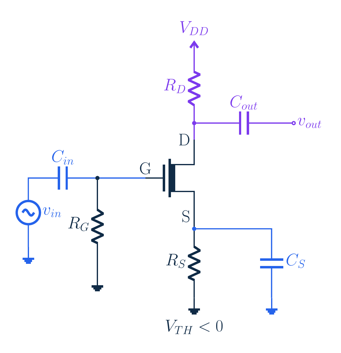
A source resistor sets the bias but disappears from the ideal bypassed AC gain. Did the capacitor remove the bias? Verify the depletion-device operating point and distinguish finite-capacitor and unbypassed models.
Written solution and narration transcript(shows the full solution)
Below are all the lines written in the notebook together with the full narration transcript.
1. A resistor with two different roles
Original same-language source. Forward motion is an independent explanatory replay, not audio-clock synchronization. Settled DC bias and small AC changes are distinct; current and voltage instruments use their stated scales. RS sets bias but disappears from ideal bypassed gain. Did the capacitor remove the bias?Separate settled source voltage from its AC change; resistor carries DC, capacitor most ACNarration transcript
A source resistor sets the operating point of this transistor. Yet the same resistor seems to disappear from the midband voltage-gain formula when a capacitor is connected across it. Did the capacitor remove the bias? Watch the steady source voltage and its small changing part separately. The resistor can still carry the steady current while the capacitor carries most of the changing current. We will explain that separation, then check both the bias and the signal in one physically possible example.
2. Keep a physically possible bias
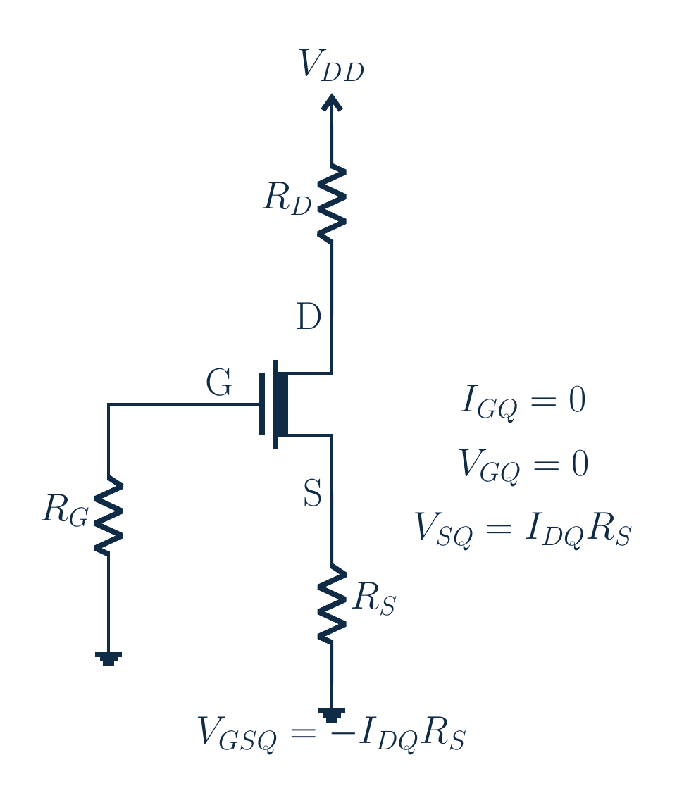
Original same-language source. Forward motion is an independent explanatory replay, not audio-clock synchronization. Settled DC bias and small AC changes are distinct; current and voltage instruments use their stated scales. Gate at DC ground; positive I_D raises source:Conducting case needs negative-threshold depletion device, not positive-threshold enhancement MOSFETNarration transcript
First inspect the actual connections. The gate resistor goes to ground and the insulated gate draws negligible steady current, so the gate is at zero DC volts. Positive drain current raises the source above ground through R S. Therefore gate-to-source voltage is negative. This conducting self-bias example needs a depletion-mode device with a negative threshold. Do not silently apply a positive-threshold enhancement MOSFET to the same grounded-gate bias and assume it is already conducting. The device model and the bias circuit must agree before we calculate a gain.
3. Keep a physically possible bias
Original same-language source. Forward motion is an independent explanatory replay, not audio-clock synchronization. Settled DC bias and small AC changes are distinct; current and voltage instruments use their stated scales. VTH=−2 V; k=1 [mA]/V² includes ½; RS=1 kΩ; ID=k(VGS−VTH)²Physical root ID=1 [mA]; VS=1 V; VGS=−1 V; reject negative-overdrive rootNarration transcript
Use a threshold of negative two volts, k of one milliamp per volt squared, and a one-kilohm source resistor. Here k already includes the factor one half. Combine I D equals k times the square of V G S minus threshold, with V G S equals negative I D R S. The physically valid solution is one milliamp. The source is at one volt and gate-to-source voltage is negative one volt. The other algebraic root would make the assumed overdrive negative, outside this branch of the device law. With twelve volts of supply and a four-point-seven-kilohm drain resistor, V D S is six point three volts, safely above the one-volt overdrive.
4. Separate DC from the changing signal
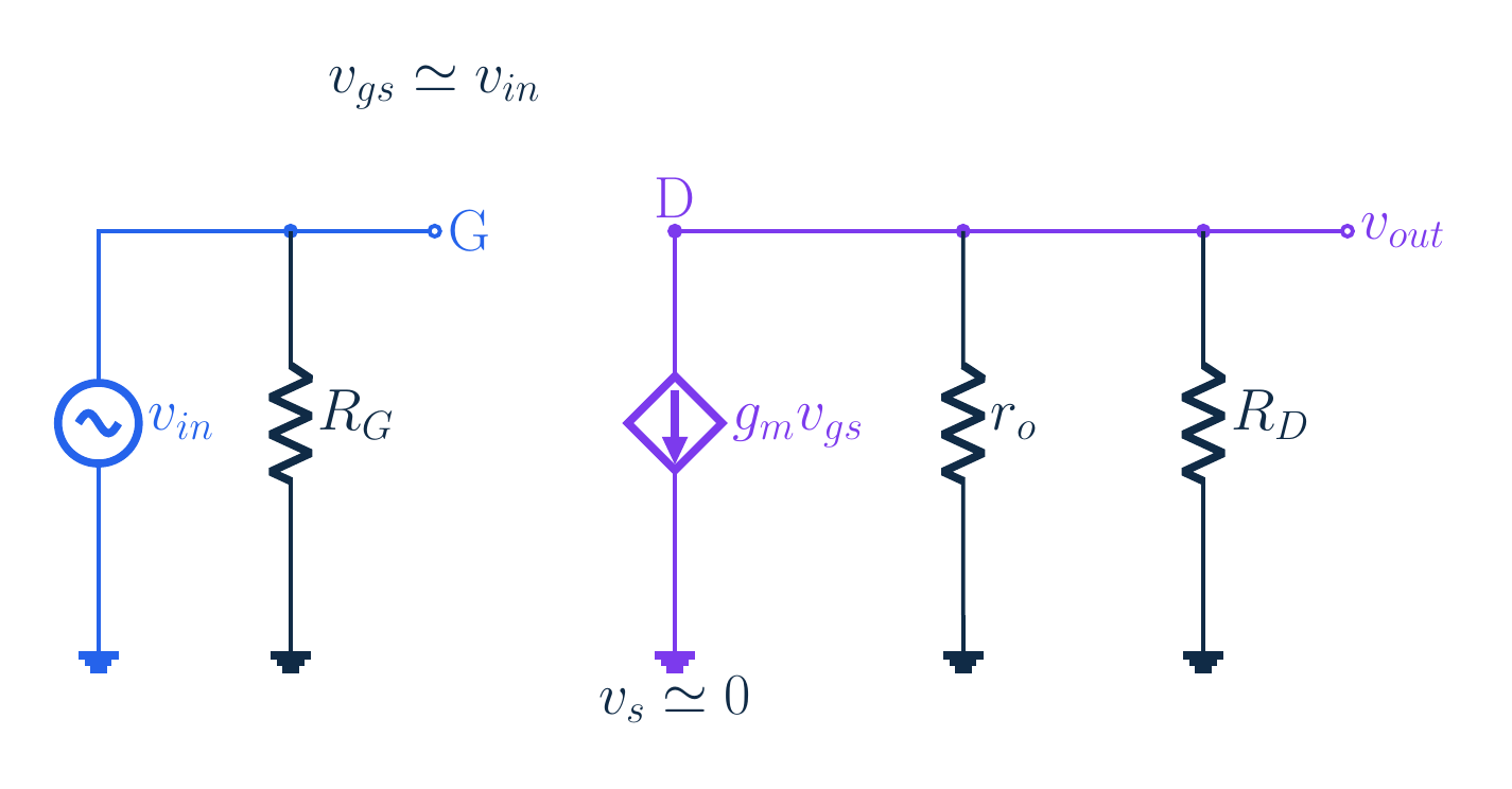
Settled DC: capacitor open; RS still sets biasMidband bypass: vs≈0 but total VS=1 V+small changeControlled source plus finite ro; output sees RD ∥ roNarration transcript
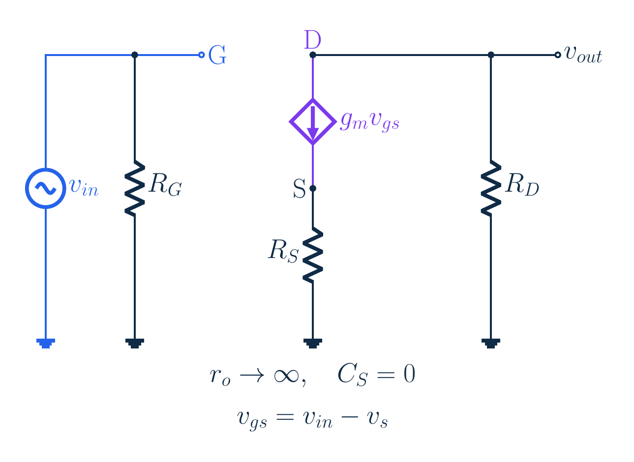
Now separate the settled bias from a small AC signal. At DC, an ideal capacitor is open after charging, so the source resistor still sets the bias current. In the bypassed midband approximation, the capacitor impedance is small enough that the changing source voltage is nearly zero. The source is at AC ground, not at zero total voltage. The total source voltage remains its one-volt bias plus a tiny changing term. Replace the transistor by its controlled current source and finite output resistance. The drain resistor and r o both connect the output to signal ground.
5. Measure the two ports and gain
Ideal gate open, but complete amplifier Rin=RG=1 MΩDevice port ≠ amplifier port; source resistance needs input dividerNarration transcript
Looking into the amplifier input, the ideal transistor gate itself takes no signal current. But the amplifier has a gate resistor to ground. A test voltage sends current through that resistor, so the input resistance is R G, not infinity. For our one-megohm gate resistor, the input resistance is one megohm under the midband assumptions. This is a useful distinction between an intrinsic device port and a complete amplifier port. If a signal generator has its own resistance, use the ordinary input divider before applying the stage gain.
6. Measure the two ports and gain
Zero input; ideal bypass makes vgs=0; Rout=RD ∥ roMeasure without external load; later RL joins gain calculation onlyNarration transcript
For output resistance, suppress the independent input signal. In the ideal bypassed model both gate and source are at AC ground, so v g s is zero and the controlled current source is zero. Apply a test voltage at the drain. Test current can flow through R D and through r o. The output resistance is R D parallel r o. This is measured with no external output load. If a load is attached later, it joins that parallel combination for the voltage-gain calculation; it is not part of the amplifier's unloaded output resistance.
7. Measure the two ports and gain
Gate↑ → drain-current control↑ → drain↓; Av≈−gm(RD ∥ ro)Bypass suppresses changing source voltage; RS still set ID and gmNarration transcript
A positive gate signal increases the controlled drain current. The drain-node voltage must fall to balance that extra current through the parallel output paths. Since v g s is approximately the input voltage in the bypassed model, output voltage is negative g m times input voltage times R D parallel r o. Divide by the input: the voltage gain is negative g m times that parallel resistance. The source resistor is absent from this AC expression because the bypass suppresses its changing voltage. Its earlier role in setting drain current and therefore g m has not disappeared.
8. Test the model with numbers
Original same-language source. Forward motion is an independent explanatory replay, not audio-clock synchronization. Settled DC bias and small AC changes are distinct; current and voltage instruments use their stated scales. ID=kVOV² → gm=2kVOV=2ID/VOV=2 mSIf law uses ½K, then K=2k; check coefficient conventionTransfer-law form: gm=2√(IDSS ID)/|VP|; use matching device/regionNarration transcript
Check the transconductance convention before substituting numbers. With I D equals k times overdrive squared, differentiation gives g m equal to two k times overdrive, also two I D divided by overdrive. Our one-milliamp current and one-volt overdrive give two millisiemens. If a textbook instead puts one half in front of its named coefficient, that coefficient is twice our k. For a JFET or a depletion-device transfer model written with I D S S and a negative pinch-off voltage, the equivalent expression is two times the square root of I D S S times I D, divided by the magnitude of pinch-off voltage. Choose the law that matches the stated device and operating region.
9. Test the model with numbers
Original same-language source. Forward motion is an independent explanatory replay, not audio-clock synchronization. Settled DC bias and small AC changes are distinct; current and voltage instruments use their stated scales. Av≈−8.592; +1 [mV] input → −8.592 [mV] outputIdeal vs=0 while DC VS=1 V; signal ground does not remove biasNarration transcript
Complete the ideal midband calculation. Four-point-seven kilohms in parallel with fifty kilohms is about four thousand two hundred ninety six point one six one ohms. Multiply by negative two millisiemens: gain is about negative eight point five nine two. A positive one millivolt input therefore gives about negative eight point five nine two millivolts output. The ideal bypassed source voltage change is zero, but its DC voltage is still one volt. That is the distinction the opening question was testing: a nearly fixed signal voltage does not imply the absence of a bias voltage.
10. Know when the bypass is an approximation


Original same-language source. Forward motion is an independent explanatory replay, not audio-clock synchronization. Settled DC bias and small AC changes are distinct; current and voltage instruments use their stated scales. C_S=100 μF at 1 [kHz]:Retain finite ZS and ro together; id=iRS+iC; vs small, not exactly zeroLower frequency weakens bypass; active source-port impedance matters, not RS aloneNarration transcript
A real capacitor is not an exact short circuit. For a one-hundred-microfarad bypass capacitor at one kilohertz, its reactance magnitude is about one point five nine two ohms. The source impedance is R S in parallel with that capacitive impedance. Our model keeps this finite impedance and r o together. At every instant, changing drain current equals changing source-resistor current plus capacitor current. The source voltage is tiny, not exactly zero, and the gain is close to the ideal bypass value. At lower frequency the bypass weakens. Comparing capacitor reactance only with R S is not a sufficient general rule; the active source-port impedance also matters.
11. Know when the bypass is an approximation
Remove capacitor only, same DC bias and finite r_o:Separate r_o→∞ approximation:Keep RG; ideal-model Rin=RG and Rout=RD; capacitor and model changes are distinctNarration transcript
Now connect this result to the unbypassed self-bias circuit. Remove only the bypass capacitor; the settled DC bias stays the same. With our finite output resistance, the unbypassed gain is about negative three point zero one nine. The original unbypassed source lesson deliberately neglects r o. Under that separate approximation, input voltage equals v g s times one plus g m R S, so gain is negative g m R D divided by one plus g m R S. Our values then give negative three point one three three. Keep the gate resistor: input resistance is R G and output resistance is R D in this infinite-r-o model. Do not confuse the change of capacitor connection with the separate change of transistor model.
12. Know when the bypass is an approximation
Original same-language source. Forward motion is an independent explanatory replay, not audio-clock synchronization. Settled DC bias and small AC changes are distinct; current and voltage instruments use their stated scales. Small signal, saturation, no body effect; RS still uses DC headroom; finite ro is independently specifiedLarge signal, coupling capacitors and external load add limits and frequency effectsNarration transcript
Keep the assumptions attached to the result: settled saturation bias, small signals, midband, negligible gate leakage and internal capacitances, and no body effect in this model. A source resistor still costs DC voltage headroom even when bypassed for AC. The local finite r o is an independently specified small-signal parameter; the simple DC square law is not a complete channel-length-modulation model. Larger signals can leave the linear region. Input coupling capacitors and the external load add their own frequency and loading effects. None of these boundaries is removed by writing a compact gain formula.
13. Know when the bypass is an approximation
Answer: resistor remains, setting bias and gm; capacitor carries most changing currentSource retains 1 V DC while +1 [mV] gate gives ≈−8.592 [mV] output; DC bias coexists with AC groundNarration transcript
Return to the apparently missing resistor. Watch the DC source voltage remain while the capacitor takes most of the changing source current. The resistor did not disappear from the circuit. It established the bias, which established g m. The capacitor made the small source-voltage change nearly zero over the intended frequency range, so the signal sees a common-source stage with gain close to negative g m times R D parallel r o. In our example the source keeps its one-volt DC bias while a one-millivolt gate signal produces an inverted output of about eight point five nine two millivolts. DC bias and AC grounding can coexist.
Source video: Electronics Basics #41 | MOSFET Bypass: AC Ground, but Still One Volt? (9:48)