Electronics 1 · Electronics Basics
#42 MOSFET divider bias: an open gate still has input loading
Question
An ideal gate takes no current. Why can only half a 1 mV source signal reach it? Follow the complete bias and signal networks, then calculate the delivered output.
Written solution and narration transcript(shows the full solution)
Below are all the lines written in the notebook together with the full narration transcript.
1. Follow the signal before the transistor

Original same-language source. Independent forward explanatory loop, not audio-clock synchronization. Signal-source resistance R_sig and MOSFET source-terminal resistor R_S are different components. Source→input network→MOSFET→output; does open gate receive all 1 [mV]?A resistor outside the transistor can attenuate the input; distinguish the two gainsNarration transcript
Start with the whole signal path: a source, the amplifier's input network, the MOSFET, and the output. The source produces one millivolt. The ideal MOSFET gate takes no signal current. Should the gate therefore receive that whole millivolt? Watch the source and gate indicators together. A resistor outside the transistor can change the answer. Our goal is to explain where the missing signal voltage appears, then predict the output without confusing the amplifier's gain with the gain of the complete source and amplifier combination.
2. Follow the signal before the transistor
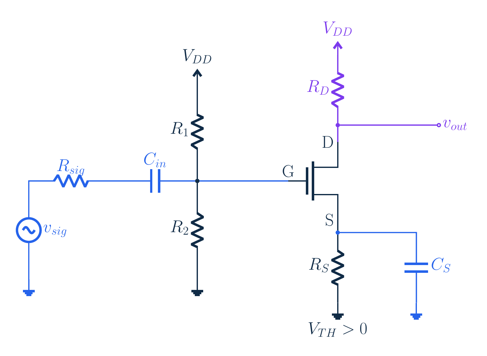
Original same-language source. Independent forward explanatory loop, not audio-clock synchronization. Signal-source resistance R_sig and MOSFET source-terminal resistor R_S are different components. R1/R2 set gate bias; RS has bypass; input coupling isolates DCRsig is external source resistance, not RS; vary Rsig without rebiasNarration transcript
R one connects the supply to the gate, and R two connects the gate to ground. The source terminal has its own resistor, R S, with a bypass capacitor in parallel. The drain connects to the supply through R D. An input coupling capacitor separates the signal source from the DC gate bias. Be careful with names: the external signal-source resistance is R sig. It is not the transistor's source-terminal resistor R S. We will change R sig while keeping this amplifier and its DC operating point unchanged.
3. Establish a valid DC operating point
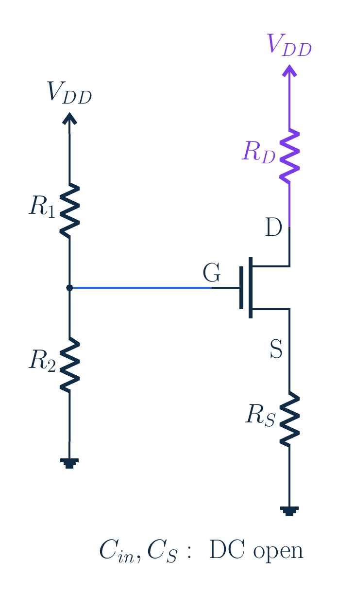
DC capacitors open; VG=12×300/(900+300)=3 VDivider current=10 [μA] despite zero gate current; separate DC from signalNarration transcript
First analyze DC, where the coupling and bypass capacitors are open circuits. Gate leakage is neglected, so the two divider resistors carry the same current. With a twelve volt supply, the gate voltage is twelve times three hundred divided by nine hundred plus three hundred: three volts. The divider current is ten microamps. Zero gate current does not mean zero current everywhere near the gate. The divider already provides a path from supply to ground. These are DC quantities; the signal changes will be calculated separately.
4. Establish a valid DC operating point
Enhancement VTH=1 V; k=1 [mA]/V² includes ½; roots ID=1 or4 [mA]4 [mA] → negative overdrive: reject; valid ID=1 [mA], VOV=1 VNarration transcript
Use an enhancement N-channel MOSFET with threshold one volt and k equal to one milliamp per volt squared. In our convention k already includes the factor one half. The source voltage is drain current times one kilohm. Substituting into the square law gives two algebraic current candidates: one and four milliamps. Test them before choosing. Four milliamps would put the source at four volts, giving a negative overdrive, so that root is not on the conducting branch of this model. The valid current is one milliamp, and the overdrive is one volt.
5. Establish a valid DC operating point
Original same-language source. Independent forward explanatory loop, not audio-clock synchronization. Signal-source resistance R_sig and MOSFET source-terminal resistor R_S are different components. Saturation check passes before small-signal linearizationNarration transcript
Now check that the assumed saturation region is consistent. One milliamp through the source resistor gives a source voltage of one volt. The gate-to-source voltage is therefore two volts. The drain resistor drops four point seven volts from the twelve volt supply, leaving seven point three volts at the drain. Subtract the source voltage: the drain-to-source voltage is six point three volts. That exceeds the one volt overdrive. The operating point is valid for our stated square-law model. We can now linearize around it instead of applying an AC gain formula to an unchecked bias.
6. Find the input and output resistances
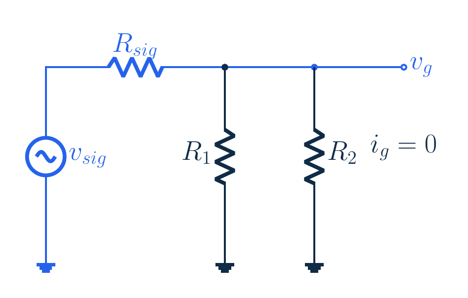
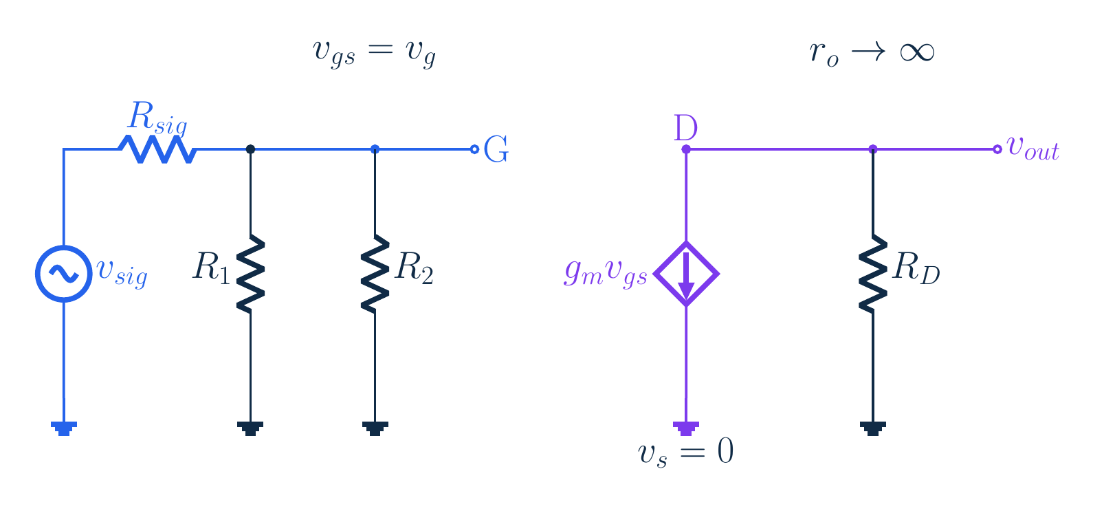
Original same-language source. Independent forward explanatory loop, not audio-clock synchronization. Signal-source resistance R_sig and MOSFET source-terminal resistor R_S are different components. Ideal midband: supply AC ground; coupling/bypass short; vs=0 but DC VS=1 Vvgs=vg; ro→∞; RS still matters in DCNarration transcript
For the ideal midband AC model, the constant supply becomes AC ground. Approximate the coupling capacitor and source bypass capacitor as shorts. This holds the changing source voltage at zero, not the total source voltage. The one volt DC bias remains. With the source fixed for AC, the gate-to-source signal equals the gate signal. We also neglect channel-length modulation, taking the transistor's output resistance as infinite. These assumptions simplify the changing circuit; they do not remove the source resistor from the earlier DC calculation.
7. Find the input and output resistances
Original same-language source. Independent forward explanatory loop, not audio-clock synchronization. Signal-source resistance R_sig and MOSFET source-terminal resistor R_S are different components. Both divider resistors lead to AC ground:900 kΩ ∥ 300 kΩ=225 kΩ; finite amplifier input, open intrinsic gateNarration transcript
Look into the amplifier input, not just into the bare gate terminal. R two already leads to ground. R one now also leads to AC ground because its other end is the fixed supply. Their signal currents add even though the gate current is zero. Therefore the amplifier input resistance is R one in parallel with R two. Nine hundred kilohms in parallel with three hundred kilohms gives two hundred twenty-five kilohms. An open gate and a finite amplifier input resistance are completely compatible. They describe different boundaries.
8. Find the input and output resistances
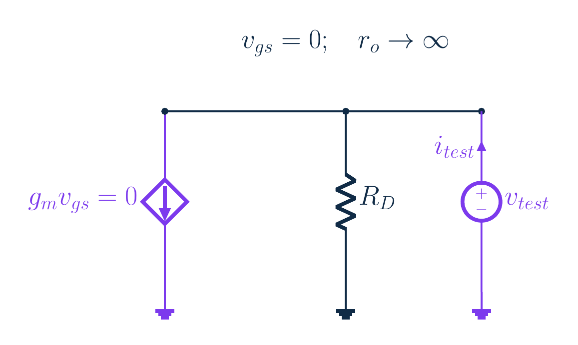
Zero independent signal, remove load, infinite r_o:External load is separate from the amplifier port resistanceNarration transcript
To find the amplifier's output resistance, suppress the independent input signal and remove any external output load. The gate and source signal voltages are then zero, so the controlled current source is zero. With infinite r o, a test voltage applied at the drain drives current only through R D. The test voltage divided by test current therefore gives R D, which is four point seven kilohms here. This is the amplifier's own output resistance. If we later attach a load, that load must be included separately when calculating the delivered output voltage.
9. Separate two different gains
Original same-language source. Independent forward explanatory loop, not audio-clock synchronization. Signal-source resistance R_sig and MOSFET source-terminal resistor R_S are different components. Gate↑ → current↑ → drain↓; Agate=−gm RDgm=2kVOV=2ID/VOV=2 mSAgate=−9.4; inversion, not negative resistanceNarration transcript
For the active signal, a positive gate change increases drain current by g m times the gate-to-source change. More drain current makes a larger drop across R D, so the drain voltage falls. The gate-to-output gain is negative g m times R D. From the square law, g m equals twice k times the overdrive, or twice the bias current divided by the overdrive. Our one milliamp and one volt give two millisiemens. Multiplying by four point seven kilohms gives a gate-to-output gain of negative nine point four. The minus sign describes inversion, not a negative resistance.
10. Separate two different gains
vg=vsig Rin/(Rsig+Rin); Asource=Agate×input fractionBias and gm unchanged; attenuation occurs before transistor; name the gain inputNarration transcript
Now restore the external signal source. Its resistance R sig and the amplifier input resistance form another voltage divider, this time for the changing signal. The gate receives R in divided by R sig plus R in times the source voltage. This attenuation comes before the transistor. Therefore the complete source-to-output gain is the gate-to-output gain multiplied by that input fraction. Nothing happened to g m or the DC bias. We changed the voltage that actually reaches the gate. Always name the input voltage in a gain ratio before comparing two reported gains.
11. Compare the same amplifier with two sources
Rsig=0: +1 [mV] source→+1 [mV] gate→−9.4 [mV] drain changeActual drain remains near 7.3 V; changing output is not a negative supplyNarration transcript
First use an ideal voltage source with zero source resistance. At the positive one millivolt source peak, the gate also receives one millivolt. The source terminal's changing voltage remains zero because of our ideal bypass assumption. Multiply the gate change by negative nine point four: the drain change is negative nine point four millivolts. Read these as changes around the operating point. The actual drain remains near seven point three volts; it has not become a negative supply voltage. The fixed scales let us compare the next experiment without a misleading automatic zoom.
12. Compare the same amplifier with two sources
Rsig=Rin=225 kΩ: +1 [mV] source→+0.5 [mV] gateSame Agate=−9.4; vo=−4.7 [mV]Other0.5 [mV] across Rsig; current enters bias resistors, not ideal gateNarration transcript
Now add two hundred twenty-five kilohms of source resistance. The amplifier input resistance has exactly the same value, so the source signal divides equally. At the same positive one millivolt source peak, the gate receives half a millivolt. The transistor stage still multiplies its gate input by negative nine point four. The drain change is therefore negative four point seven millivolts. The other half millivolt is across the external source resistor. Current flows through the two bias resistors, not into the ideal gate. This is ordinary input loading, despite the insulated gate.
13. Answer the question and state the limits
Original same-language source. Independent forward explanatory loop, not audio-clock synchronization. Signal-source resistance R_sig and MOSFET source-terminal resistor R_S are different components. Finite ro/load reduce drain resistance; finite bypass/coupling and gate capacitance limit bandSmall signal, fixed saturation bias; keep device-specific gm conventions separateNarration transcript
The compact gain formula has boundaries. A finite transistor output resistance reduces the effective drain resistance, and an external load reduces it further. A real bypass capacitor does not short the source at every frequency, so source feedback returns when its impedance matters. Coupling and gate capacitances also limit the useful frequency range. We assumed small signals and a fixed saturation bias, not clipping or thermal drift. Saying r o is much larger than R D is an approximation, not an exact equality. Keep the source note's device-specific transconductance formulas separate rather than mixing enhancement and depletion parameters.
14. Answer the question and state the limits
Answer: bias resistors draw signal current; equal input/source resistances give 1→0.5→−4.7 [mV]Source terminal retains1 V DC and zero ideal AC; follow the entire networkNarration transcript
Return to the source and gate indicators. Why did half the signal fail to reach an ideal gate that takes no current? Because the amplifier input includes its bias resistors. Their parallel resistance and the external source resistance form a divider. With equal resistances, one millivolt at the source becomes half a millivolt at the gate, then negative four point seven millivolts at the drain. The source terminal keeps its one volt DC bias while its ideal bypassed signal change stays zero. Follow the whole network, name the voltage used in your gain ratio, and the apparently missing half of the signal is accounted for.
Source video: Electronics Basics #42 | Zero Gate Current, Half the Signal? MOSFET Input Divider (9:51)