Electronics 1 · Electronics Basics
#43 Source follower: useful buffering with gain below one
Question
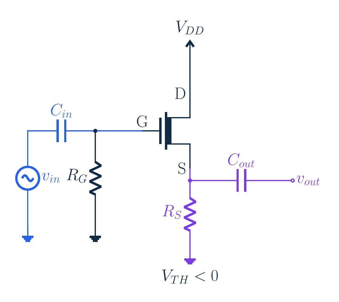
Why insert an amplifier with voltage gain below one between a weak source and a load? Compare the voltage actually delivered to the same load directly and through a source follower.
Written solution and narration transcript(shows the full solution)
Below are all the lines written in the notebook together with the full narration transcript.
1. A useful amplifier with gain below one
Original same-language source. Held experiment frame or schematic; no artificial movement is added. The displayed result follows its completed calculation. Local finite-ro model, not a full transistor simulation. Gain below1: why insert a follower rather than connect the load directly?Compare delivered voltage to the same load, not unloaded transistor gainNarration transcript
A voltage amplifier with gain below one sounds disappointing. Why place it between a signal source and a load? Start with the whole task: deliver a signal to that load. We can connect the load directly, or insert a source follower. The useful comparison is the voltage that actually reaches the same load in both arrangements, not the unloaded gain written beside the transistor. We will see how taking little current from the input and providing a lower output resistance can make the second arrangement much more useful.
2. A useful amplifier with gain below one
Original same-language source. Held experiment frame or schematic; no artificial movement is added. The displayed result follows its completed calculation. Local finite-ro model, not a full transistor simulation. Gate input, source output; drain AC ground; RS must not be bypassedRG is DC return; coupling isolates external source/load from bias; common drainNarration transcript
In a source follower, the gate is the input and the source terminal is the output. The drain connects directly to the fixed supply, which becomes AC ground in the small-signal model. R S connects the source to ground. It is not bypassed here, because the changing source voltage is precisely our output. R G supplies the gate's DC return path. Input and output coupling capacitors separate the external signal source and load from the DC bias. This arrangement is also called common drain: the drain is the common signal reference.
3. The output follows through feedback
Original same-language source. Held experiment frame or schematic; no artificial movement is added. The displayed result follows its completed calculation. Local finite-ro model, not a full transistor simulation. Depletion device: VTH=−2 V; k=1 [mA]/V² includes½; RS=1 kΩ; VDD=12 Vgm=2 mS; independently specified local ro=50 kΩNarration transcript
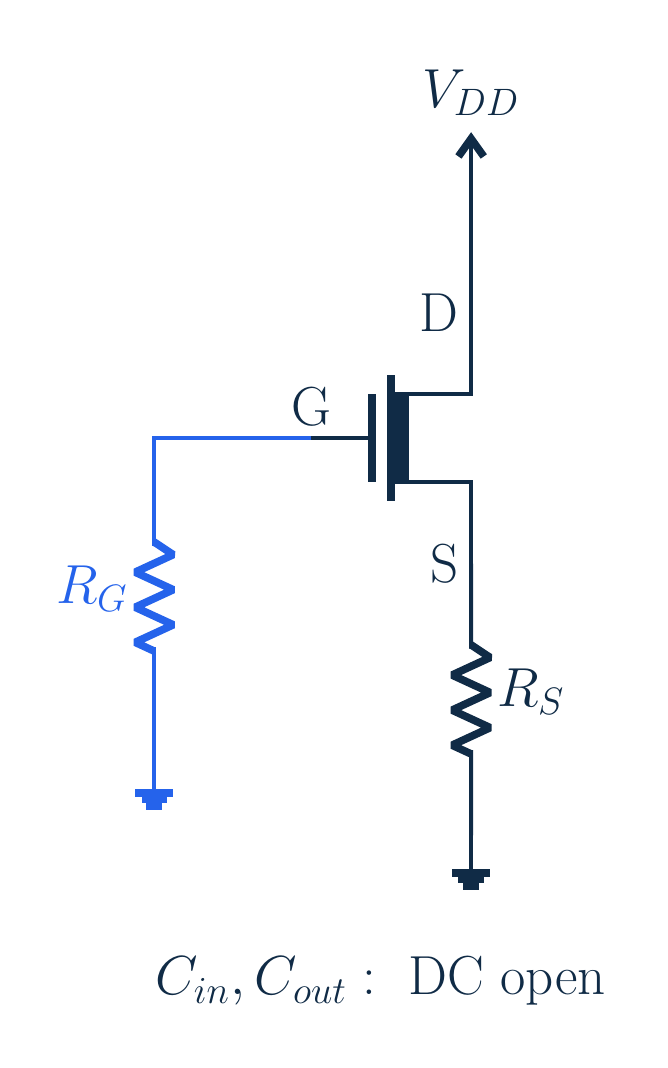
Our supplemental example uses a depletion N-channel MOSFET, because a gate tied to zero DC with a positive source voltage needs a negative threshold to conduct. Choose threshold negative two volts, k of one milliamp per volt squared, R S of one kilohm and supply twelve volts. K includes the factor one half. The valid square-law bias gives one milliamp, source voltage one volt and gate-to-source voltage negative one volt. The drain-to-source voltage is eleven volts, safely above the one volt overdrive. The local transconductance is two millisiemens. We separately specify local output resistance as fifty kilohms.
4. The output follows through feedback
Gate↑ → source↑ → controlling vgs reduced: negative feedbackvg=vgs+vo; RS ∥ ro to AC ground; output follows but by lessNarration transcript
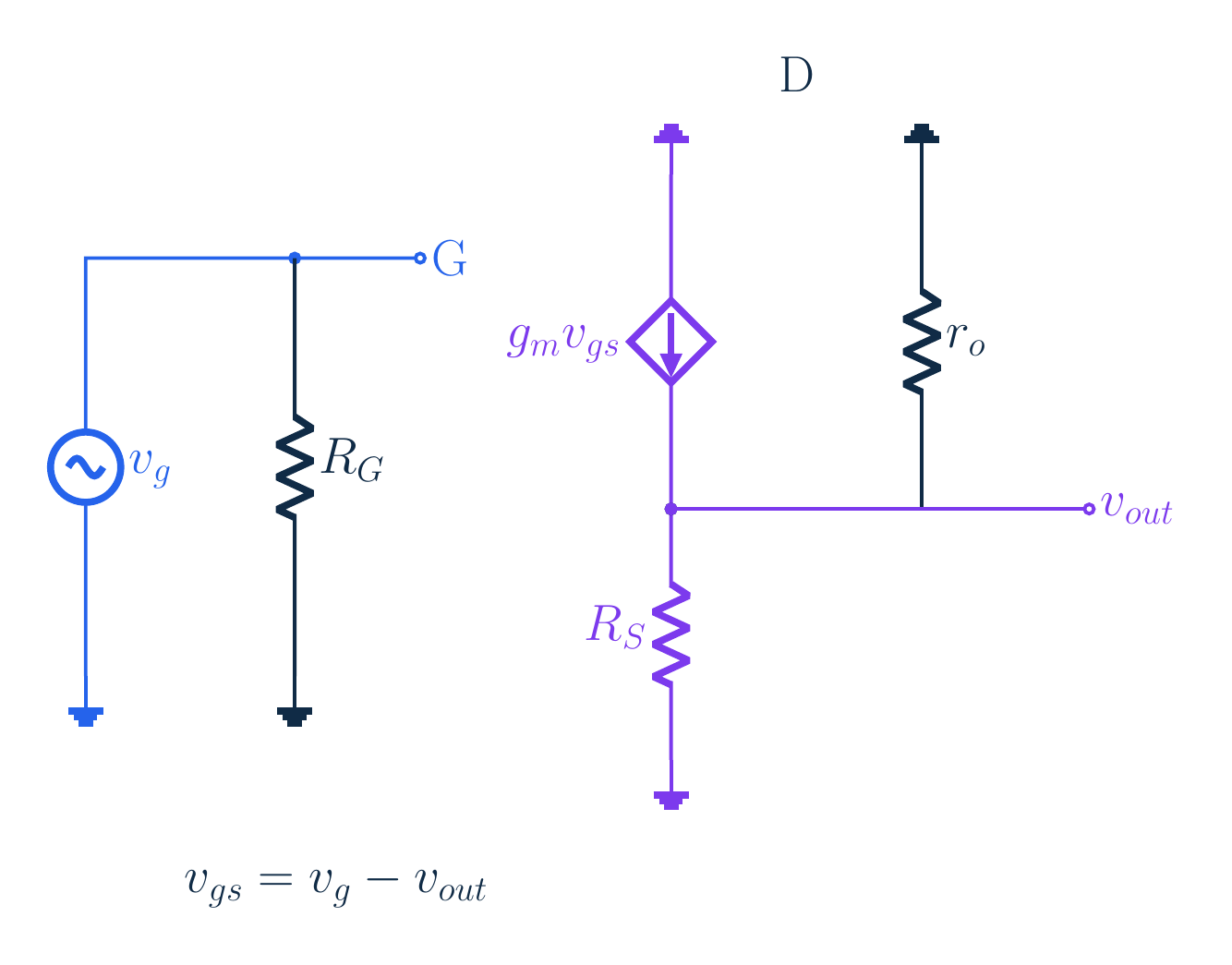
Now raise the gate signal. The controlled drain current tends to rise, which raises the source voltage across R S. But that source rise subtracts from the gate-to-source change that caused it. This is local negative feedback. The gate signal equals the gate-to-source signal plus the output. Keep finite r o in the model: because the drain is AC ground, r o and R S both connect the output to signal ground. The output follows in the same direction as the gate, but by a smaller amount. The transistor responds to a voltage difference, not to the gate voltage alone.
5. The output follows through feedback
Av=gm/(gm+1/RS+1/ro); 0<Av<1; finite ro retainedNarration transcript
Call R S in parallel with r o the effective source resistance. The controlled current times that resistance gives the output. Substitute gate signal minus output for the gate-to-source signal, then collect the output terms. The gain becomes g m times the effective resistance divided by one plus that same product. Equivalently, it is g m divided by g m plus one over R S plus one over r o. All these conductances are positive, so the gain is positive and below one. Infinite r o is a separate limiting approximation; it is not the finite-resistance circuit we just derived.
6. High input, low output resistance
Original same-language source. Held experiment frame or schematic; no artificial movement is added. The displayed result follows its completed calculation. Local finite-ro model, not a full transistor simulation. Whole amplifier Rin=RG=1 MΩ, not bare open gateExternal Rsig=100 kΩ still divides input; RG, RS and Rsig have different jobsNarration transcript
The ideal MOS gate takes no signal current, but the amplifier input includes R G. With our midband coupling approximation, the input resistance is therefore R G. We choose one megohm. An external source resistance still forms an input divider with that megohm; insulated gate does not mean zero loading by the whole circuit. In the practical comparison we will use one hundred kilohms of source resistance, so most, but not all, of the source voltage reaches the gate. R G, R S and the external source resistance are three different resistors with different jobs.
7. High input, low output resistance
Original same-language source. Held experiment frame or schematic; no artificial movement is added. The displayed result follows its completed calculation. Local finite-ro model, not a full transistor simulation. Remove load, zero gate input; keep dependent source:Narration transcript
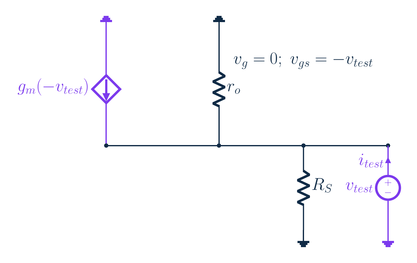
For output resistance, remove the external load and suppress the independent gate input. Do not turn off the dependent current source. Apply a test voltage at the source output. The gate is at zero signal, so the gate-to-source voltage is negative the test voltage, not zero. The required test current is the test voltage times one over R S plus one over r o plus g m. Output resistance is therefore the parallel combination of R S, r o and one over g m. With our values, it is about three hundred thirty-one point one ohms. The dependent source is why the result is lower than R S alone.
8. Compare the same source and load
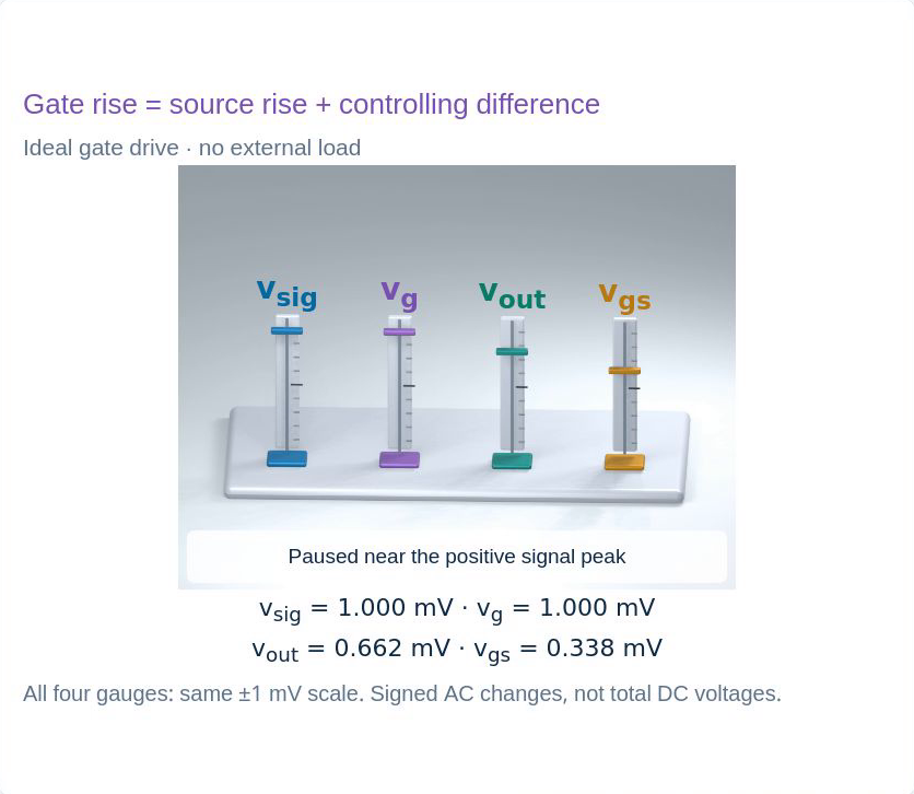
Original same-language source. Held experiment frame or schematic; no artificial movement is added. The displayed result follows its completed calculation. Local finite-ro model, not a full transistor simulation. Unloaded denominator=2+1+0.02=3.02 mS; Av≈+0.662+1 [mV] gate→+0.662 [mV] source; remaining vgs≈0.338 [mV]Source follows without reaching gate change; all are AC changes around biasNarration transcript
First drive the gate with an ideal voltage source and leave the external output load disconnected. The denominator in the conductance form is two plus one plus zero point zero two millisiemens. Dividing two by three point zero two gives a positive gain of about zero point six six two. A positive one millivolt gate change therefore gives about positive zero point six six two millivolts at the source output. The remaining gate-to-source change is about zero point three three eight millivolts. Watch how the source follows without reaching the whole gate change. All these are small changes around the existing bias.
9. Compare the same source and load
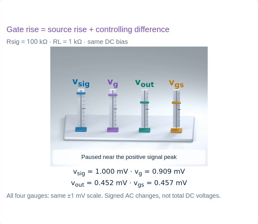
Original same-language source. Held experiment frame or schematic; no artificial movement is added. The displayed result follows its completed calculation. Local finite-ro model, not a full transistor simulation. R_L=1 kΩ adds1 mS:Rsig=100 kΩ; RG=1 MΩ → gate fraction=10/11Same1 [mV] source→load≈+0.452 [mV]; coupling preserves DC biasNarration transcript
Now connect a one kilohm AC-coupled load. It adds one more millisiemens at the source output, making the gate-to-output gain two divided by four point zero two, about zero point four nine eight. Add the one hundred kilohm signal-source resistance at the input. With R G of one megohm, the gate receives ten elevenths of the source signal. Multiply the two factors. A positive one millivolt source signal gives about positive zero point four five two millivolts across the load. Neither coupling capacitor changes the DC operating point in this ideal midband comparison.
10. Compare the same source and load
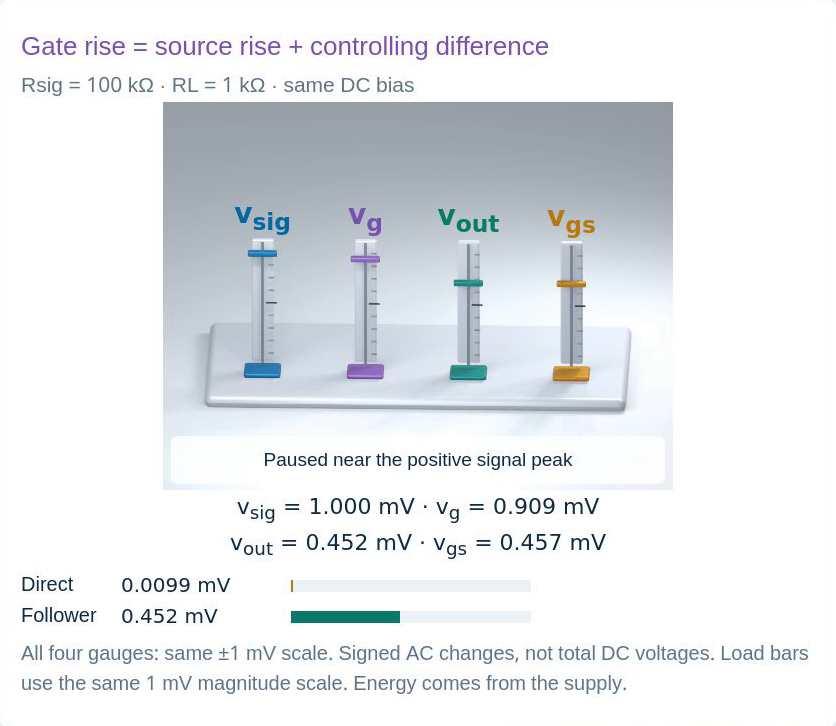
Original same-language source. Held experiment frame or schematic; no artificial movement is added. The displayed result follows its completed calculation. Local finite-ro model, not a full transistor simulation. Direct100 kΩ source→1 kΩ load: fraction=1/101; vload≈0.0099 [mV]Follower delivers≈0.452 [mV], over40× direct, although its own gain<1Isolates weak source from heavy load; energy comes from DC supplyNarration transcript
Compare that with removing the follower and connecting the same one hundred kilohm source resistance directly to the same one kilohm load. The load receives one divided by one hundred and one of the source signal: about zero point zero zero nine nine millivolts for our one millivolt source. The follower delivers about zero point four five two millivolts instead, over forty times as much in this example. Its own voltage gain is still below one. It helps because it isolates the weak source from the heavy load. The energy delivered to the load is supported by the DC supply, not created by a passive divider.
11. What the follower can and cannot do
Not ideal voltage source: gain<1, nonzero Rout, finite current/headroom; saturation can failBody effect/leakage/capacitance omitted; local finite-ro model has frequency and bias limitsNarration transcript
A source follower is not an ideal voltage source. Its gain stays below one, its output resistance is nonzero, and heavier loads reduce the output further. Available current and voltage headroom are limited. Large excursions can leave the assumed saturation region. Real devices can also have body effect, leakage and capacitance, all excluded from our displayed local model. The original note retains finite r o, so we did too. The square-law bias example and independently stated local r o are an explanatory approximation, not a complete transistor simulation. Check frequency range and operating point before extending these results.
12. What the follower can and cannot do
Answer: same load gets0.0099 [mV] direct versus0.452 [mV] bufferedHigh input resistance, lower output resistance; objective is useful loaded signal, not large unloaded gainNarration transcript
Return to the opening question: why use a stage with voltage gain below one? Look at the same load in our two arrangements. Direct connection delivered about zero point zero zero nine nine millivolts; the follower delivered about zero point four five two millivolts. Its high input resistance avoids severe source loading, while source feedback produces a lower output resistance. Inside the follower, the source rises with the gate but by less, leaving the gate-to-source difference that drives the needed current. The practical objective was not a large unloaded gain. It was a useful signal across a real load.
Source video: Electronics Basics #43 | Gain Below One: Why Use a MOSFET Source Follower? (8:48)