Electronics 1 · Electronics Basics
#44 Common-gate MOSFET: fixed gate, rising drain
Question
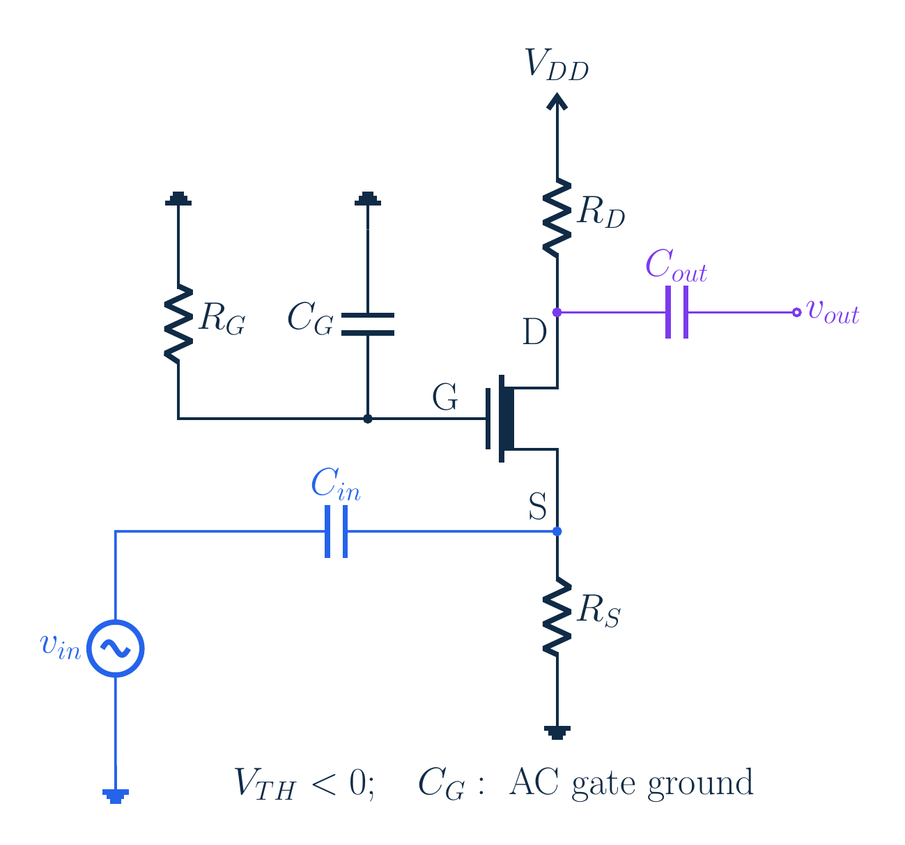
Keep the gate at AC ground and apply the input at the source. Why does a positive source signal raise the drain output, and why does this insulated-gate transistor have low amplifier input resistance?
Written solution and narration transcript(shows the full solution)
Below are all the lines written in the notebook together with the full narration transcript.
1. Move the source, not the gate
Original same-language source. Independent forward explanatory replay, not audio-clock synchronized. Source is the signal input; gate AC ground is distinct from DC bias. Can a fixed gate still amplify? Input at source; output at drain; gate is common referenceRaise source: predict drain direction and why the input draws currentNarration transcript
Can a MOSFET amplify a signal while its gate is held still? First identify the three terminals. Today the signal enters the source, and the output is taken from the drain. The gate is our fixed signal reference. Imagine raising the source by a tiny amount. Will the drain output rise or fall? We will follow the gate-to-source voltage, the drain-current change and the drain-resistor drop to answer that question. Then we will explain why this source input draws current even though the MOS gate itself is insulated.
2. Move the source, not the gate
Original same-language source. Independent forward explanatory replay, not audio-clock synchronized. Source is the signal input; gate AC ground is distinct from DC bias. RD to supply, RS to ground; couple into source and out of drain; gate AC-groundedAC ground≠zero DC; do not bypass RS because that would short the inputNarration transcript
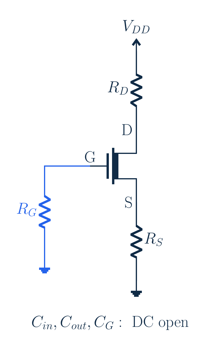
The drain resistor R D connects to the supply. R S connects the source to ground, and the input signal is coupled into that source node. The output is coupled from the drain. A capacitor holds the gate at AC ground over the frequency range of interest. AC ground does not require zero DC gate voltage; those are different statements. In our supplemental bias example the gate's DC return happens to go to ground too. Do not place a bypass capacitor across R S here: that would also short the source input we are trying to drive.
3. Follow the control voltage and signs
Original same-language source. Independent forward explanatory replay, not audio-clock synchronized. Source is the signal input; gate AC ground is distinct from DC bias. Depletion VTH=−2 V; k=1 [mA]/V² includes½; RS=1 kΩ; RD=4.7 kΩ; VDD=12 VVDS>VOV=1 V; gm=2 mS; neglect ro and body effectNarration transcript
Use a depletion N-channel MOSFET for this grounded-DC-gate example. Choose threshold negative two volts, k of one milliamp per volt squared, source resistor one kilohm, drain resistor four point seven kilohms and supply twelve volts. K includes one half in the square law. The valid bias current is one milliamp. The source is at one volt and the gate-to-source voltage is negative one volt. The drain is at seven point three volts, so drain-to-source voltage is six point three volts. This exceeds the one volt overdrive and gives local g m of two millisiemens. We neglect r o and body effect in the AC model.
4. Follow the control voltage and signs
Original same-language source. Independent forward explanatory replay, not audio-clock synchronized. Source is the signal input; gate AC ground is distinct from DC bias. Source↑ → vgs↓ → drain current↓ → RD drop↓ → drain↑Narration transcript

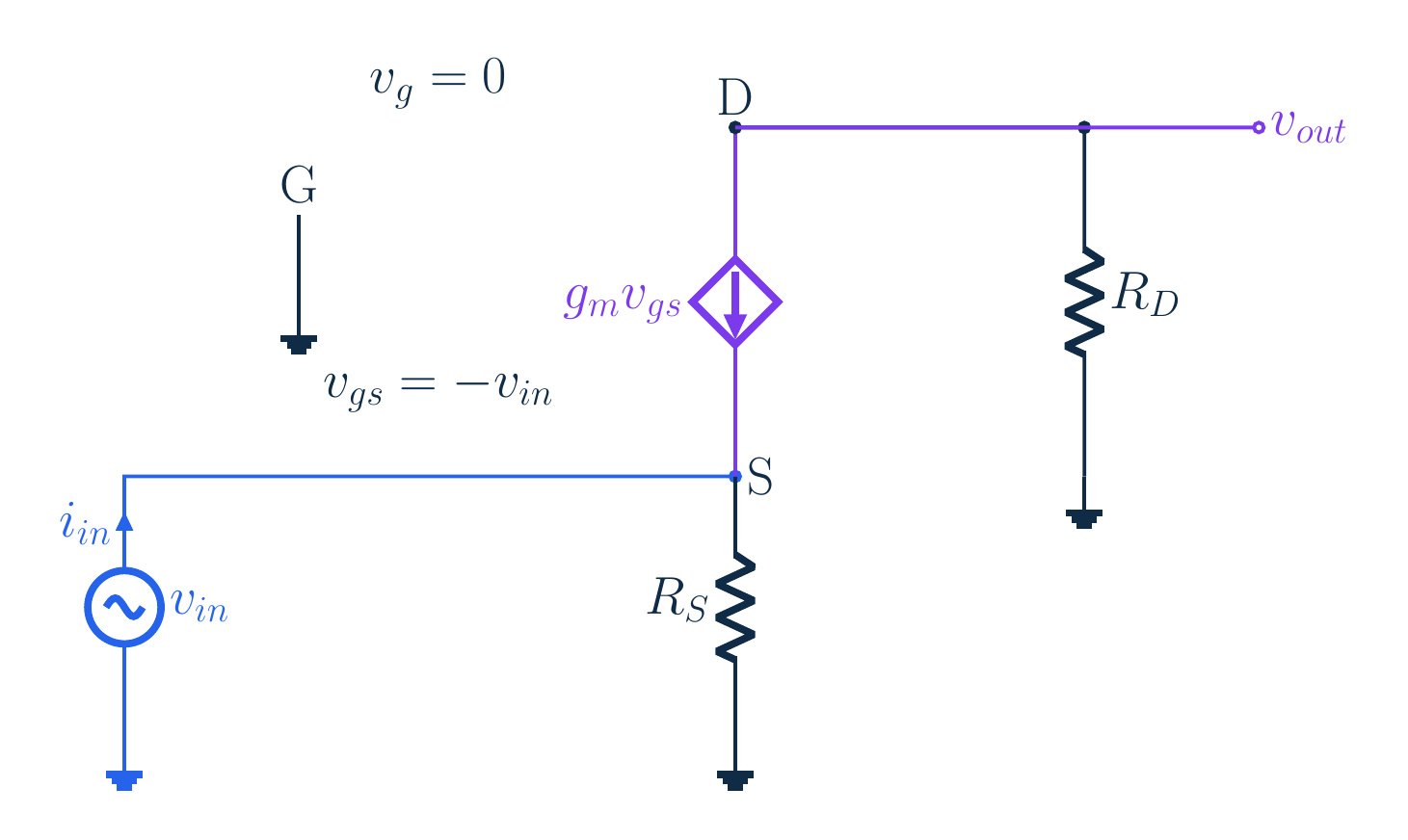
The controlling voltage is gate minus source. Since the gate change is zero and the source change is our input, the gate-to-source signal equals negative the input. A positive source input therefore reduces the controlling voltage. The drain-current change is g m times that negative change, so it decreases. Less drain current means less voltage drop across R D. The drain output rises. Nothing reversed the transistor's control law: we moved the other end of the controlling voltage difference. This is the origin of the positive common-gate voltage gain.
5. Follow the control voltage and signs
Infinite ro, no external load; add RD ∥ RL for loaded gain, not own RoutNarration transcript
Write the same sign argument as equations. The drain-current change is g m v g s, which is negative g m v in. The output change is negative drain current times R D. The two minus signs cancel, leaving positive g m R D times the input. Hence the stage gain is positive g m times R D. This formula assumes no external output load and an infinite transistor output resistance. If a separate AC load is connected, use R D in parallel with that load for the delivered voltage gain. Do not silently count the load as part of the amplifier's own output resistance.
6. Why the source input draws current
Original same-language source. Independent forward explanatory replay, not audio-clock synchronized. Source is the signal input; gate AC ground is distinct from DC bias. Input is source, not gate:Narration transcript
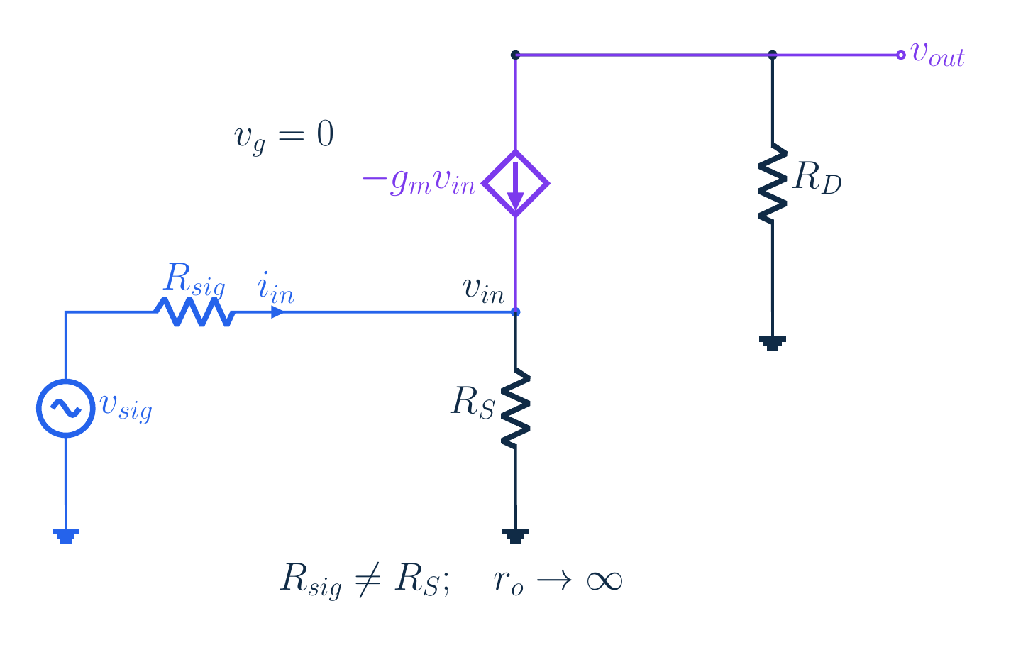
Why is the input resistance not enormous if the gate is insulated? Because the input terminal is the source, not the gate. At the source node, the incoming signal current plus the drain-current change equals the current through R S. Substitute negative g m times the input for the drain-current change. The required input current is input voltage times one over R S plus g m. Dividing voltage by current gives R S in parallel with one over g m. In our example, one kilohm in parallel with five hundred ohms is about three hundred thirty-three point three ohms.
7. Why the source input draws current
Zero independent input, remove load; vgs=0 makes dependent current zero by its lawRout=RD=4.7 kΩ; source-follower output test is differentNarration transcript
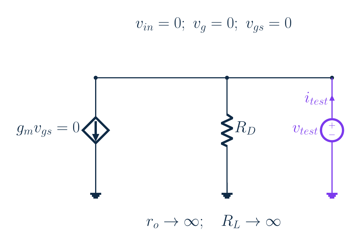
For output resistance, suppress the independent source input and remove any external output load. The gate and source signals are then zero. In this infinite r o model, a test voltage at the drain cannot feed back through a drain-to-source resistance. The controlled source evaluates to zero because its controlling voltage is zero, not because dependent sources may always be turned off. The test current flows through R D. Output resistance is therefore R D, or four point seven kilohms here. This reasoning differs from the source follower, where an output test directly changes the source and hence v g s.
8. Check a complete signal example
Original same-language source. Independent forward explanatory replay, not audio-clock synchronized. Source is the signal input; gate AC ground is distinct from DC bias. ΔiRS=+1 [μA]; required iin=+3 [μA]Total ID≈0.998 [mA] remains positive; gain and input resistance agreeNarration transcript
Apply positive one millivolt directly at the source input. The gate stays fixed, so v g s changes by negative one millivolt. With g m of two millisiemens, the drain-current change is negative two microamps. Multiply by negative four point seven kilohms: the drain output changes by positive nine point four millivolts. Meanwhile the source resistor carries an incremental one microamp to ground. The input source must supply three microamps to satisfy the source-node balance. The total drain current remains about zero point nine nine eight milliamps, still positive. These measurements simultaneously verify the gain and input resistance.
9. Check a complete signal example
External Rsig=1 kΩ with Rin≈333.3 Ω → input fraction=1/41 [mV] generator→0.25 [mV] transistor input→+2.35 [mV] output; stage gain still+9.4Narration transcript
The low input resistance makes external source resistance important. Add one kilohm of signal-source resistance, R sig, outside the amplifier. It forms a divider with the approximately three hundred thirty-three ohm input resistance. Only one quarter of the source voltage reaches the source terminal. A one millivolt signal generator therefore gives a quarter millivolt at the transistor input. The stage still multiplies its own input by positive nine point four, so the output is positive two point three five millivolts. Overall gain and stage gain differ because their denominators refer to different voltages.
10. Compare the three common arrangements
CS: gate→drain, inverts; CD: gate→source, positive<1; CG: source→drain, positiveCommon-gate input is not insulated gate; identify ports before signs and currentsNarration transcript
Place the three familiar arrangements side by side and first mark input, output and common terminal. Common source receives the gate signal and produces an inverted drain output. Common drain receives the gate signal and lets the source follow, with positive voltage gain below one in the model we studied. Common gate receives the source signal and produces a noninverted drain output. The insulated gate is not the input terminal in this last arrangement. Terminal choice changes both the gain sign and the input-current requirement. A transistor name alone is not enough to identify amplifier behavior.
11. Compare the three common arrangements
Original same-language source. Independent forward explanatory replay, not audio-clock synchronized. Source is the signal input; gate AC ground is distinct from DC bias. Infinite ro and no body effect; real source input can alter body voltage and conductanceGrounding/coupling has frequency limits; small-signal saturation/headroom assumptions remainNarration transcript
Our compact formulas assume infinite r o, no body effect, a fixed saturation bias and small signals. A real source input may change the body-to-source voltage too, so body effect can alter the effective input conductance and gain. Finite r o also couples the output and input differently. Gate grounding and coupling capacitors work only over their intended frequency range. Large signals can violate the local approximation or available voltage headroom. We are explaining the original note's ideal model, not claiming a full-frequency or large-signal transistor simulation. State those boundaries before reusing the formulas.
12. Compare the three common arrangements
Answer: fixed gate, source↑ → controlling voltage↓ → drain current↓ → drain↑; +1 [mV]→+9.4 [mV] at3 [μA] inputControl is a difference between terminals; follow ports and signsNarration transcript
Return to the gate held still. Raise the source input: the gate-to-source voltage falls, drain current falls, and the drain voltage rises. Our positive one millivolt source-terminal input produced positive nine point four millivolts at the drain. It required three microamps of input current, consistent with roughly three hundred thirty-three ohms of input resistance. The gate can stay still while the transistor amplifies because the controlling quantity is a difference between two terminals. Identify those terminals, follow the signs through the model, and common-gate gain no longer looks like an exception.
Source video: Electronics Basics #44 | Gate Held Still, Output Rises? Common-Gate MOSFET (8:52)