Digital Design · NAND and NOR Universal Gates
#07 Build NOT, AND and OR from one gate family, then verify a three-NAND implementation of a Boolean function
Reconstruct basic operations using only NAND or only NOR gates, then check every row of a worked three-gate circuit.
Question

Work with ideal two-input gates and independent binary variables A, B and C. Plus denotes inclusive Boolean OR, a dot denotes AND, and a prime denotes the complement of its complete operand or parenthesized group. Prime is not differentiation; Boolean OR is not ordinary integer addition. Juxtaposed AB means A AND B. A gate family is functionally complete when networks of sufficiently many gates from that family can implement any finite Boolean function. This does not mean that one isolated gate implements every function. NOT, AND and OR suffice because a truth table can be expressed as an OR of product terms. Constant functions are included: A AND NOT A gives zero, and A OR NOT A gives one when an input is available. The output bubble in a NAND or NOR symbol represents inversion. Tie both inputs of a NAND to A: (A·A)'=A'. Tie both inputs of a NOR to A: (A+A)'=A'. Each junction dot means both input pins are connected to the same electrical node. They are not two independent signals and neither pin is left floating. To obtain AND with two NAND gates, define X=(A·B)' and feed X to both inputs of another NAND; its output is (X·X)'=X'=A·B. To obtain OR with two NOR gates, define X=(A+B)' and invert X using tied inputs of another NOR; the output is A+B. NAND-only OR is obtained by separately inverting A and B and NANDing the two complements: (A'·B')'=A+B. NOR-only AND is similarly (A'+B')'=A·B. Each construction uses as many repeated gates as required; no separate inverter symbol is needed. For the worked target F=A·B+C, let N₁=(A·B)' and N₂=(C·C)'=C'. The final NAND receives the separate signals N₁ and N₂, giving F=(N₁·N₂)'=((A·B)'·C')'=A·B+C. The phrase A B prime in the substitution refers to the complement of the complete product AB, as already defined by N₁; write the parentheses explicitly. It does not mean A·B'. The final NAND wires are separate input nodes; do not short N₁ and N₂ together. Read assignments in binary order 000, 001, 010, 011, 100, 101, 110, 111. The A·B column is 0,0,0,0,0,0,1,1. N₁ is 1,1,1,1,1,1,0,0; N₂ is 1,0,1,0,1,0,1,0. Both direct F and circuit F are 0,1,0,1,0,1,1,1. If C=1, F=1 for all A,B. If C=0, F=A·B. The last two rows have A=B=1 and F=1 regardless of C. With all three inputs one, Boolean OR still produces one, not the integer sum two. The source's complete row-by-row agreement establishes the ideal steady Boolean function for every input assignment. It does not establish propagation delays, analog voltage limits, loading, power, transistor count, absence of transient hazards or full physical circuit qualification. Three NAND gates suffice for the shown example; no general claim of minimum area or minimum gate count is needed. Decoders and encoders are only the next-topic preview.
Written solution and narration transcript(shows the full solution)
Below are all the lines written in the notebook together with the full narration transcript.
1. Define a universal gate family
Output bubbles indicate complementation. Tied inputs share a junction; the two inputs of the final NAND in the worked circuit remain distinct. The direct expression A·B OR C and the three-NAND output agree for all eight binary assignments. A universal gate family can implement every Boolean function.NOT, AND and OR form a complete set of operations.Reconstruct these three operations using gates from just one family.NAND output:NOR output:The small output circle represents inversion.The bubble changes the gate operation; it is part of the circuit symbol.Narration transcript
A gate family is universal, or functionally complete, when it can build every Boolean function. We already know that NOT, AND, and OR can describe any Boolean expression. So the proof strategy is practical: use one gate family to reconstruct those three operations. NAND starts as AND and then inverts its output. NOR starts as OR and then inverts its output. In both symbols, the small circle at the output is the inversion bubble. It is an electrical operation, not decoration.
2. Build an inverter from tied inputs
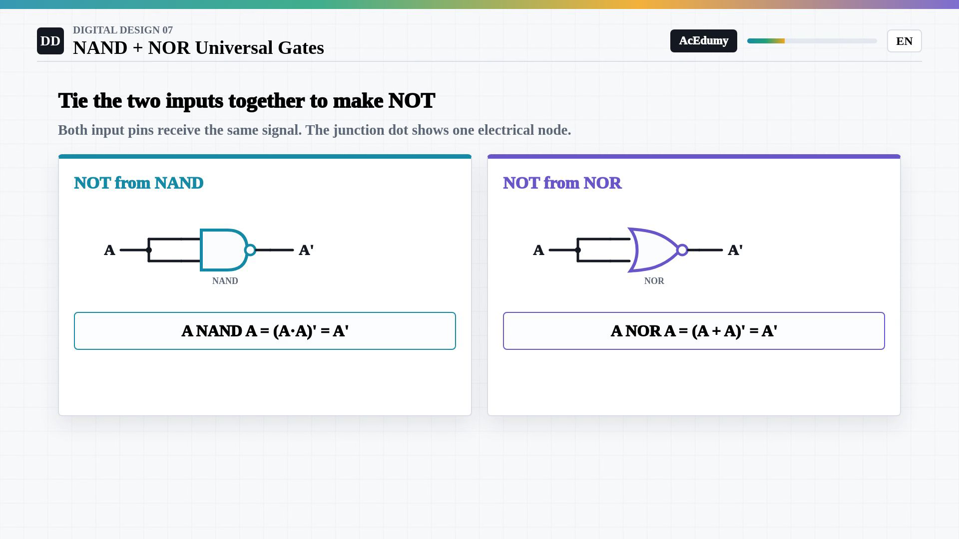
Output bubbles indicate complementation. Tied inputs share a junction; the two inputs of the final NAND in the worked circuit remain distinct. The direct expression A·B OR C and the three-NAND output agree for all eight binary assignments. Build an inverter by tying two inputs together.Connect both NAND input pins to the same signal A.Tied NAND output:Idempotence gives:Tied NOR output:A junction dot identifies the shared electrical node feeding both pins.Either construction uses one gate to implement NOT.Narration transcript
The first construction is an inverter. Connect both inputs of a NAND gate to the same signal A. The gate computes the complement of A AND A. Since A AND A equals A, the output is A prime. The same idea works with NOR: A OR A also equals A, and NOR complements it. In the schematics, the junction dot shows that both input pins belong to the same electrical node. One NAND or one NOR can therefore reproduce NOT.
3. Recover AND and OR
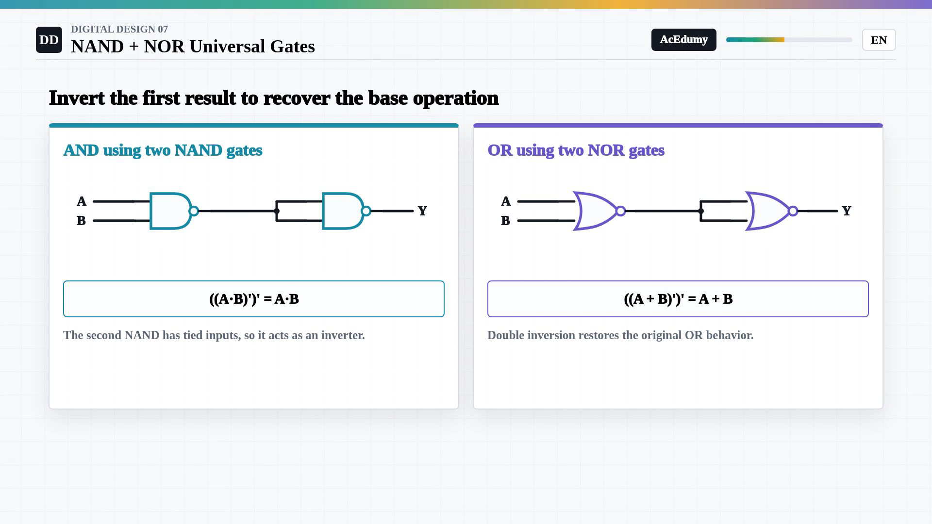
Output bubbles indicate complementation. Tied inputs share a junction; the two inputs of the final NAND in the worked circuit remain distinct. The direct expression A·B OR C and the three-NAND output agree for all eight binary assignments. Recover each family's original operation with a second inversion.First NAND output:Tied second NAND:Double complement:Two NAND gates implement AND.Use the corresponding construction with NOR gates.First NOR output:Double complement:De Morgan transformations supply the remaining operation.Narration transcript
Now recover each family's base operation. A first NAND produces the complement of A AND B. Feed that result into both inputs of a second NAND, which acts as an inverter. Double inversion leaves A AND B. Two NAND gates therefore reproduce AND. The NOR construction is parallel. A first NOR produces the complement of A OR B, and a tied-input NOR inverts that result again. The output is A OR B. With NOT plus the recovered operation, De Morgan's laws can supply the remaining operation.
4. Implement a function with three NAND gates
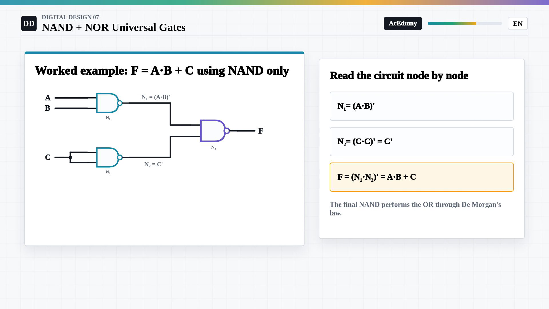
Output bubbles indicate complementation. Tied inputs share a junction; the two inputs of the final NAND in the worked circuit remain distinct. The direct expression A·B OR C and the three-NAND output agree for all eight binary assignments. Target Boolean function:Identify each internal node before simplifying the final output.First node:Second node:Connect N₁ and N₂ to the two distinct inputs of the final NAND.Final NAND output:Substitute complete node expressions:Apply De Morgan and double complementation:The complete circuit contains three NAND gates.Narration transcript
Let us implement F equals A B plus C using NAND gates only. Read the circuit node by node. N one is NAND of A and B, so N one equals the complement of A B. N two has both inputs tied to C, so it acts as an inverter and produces C prime. The final NAND receives N one and N two. Its output is the complement of their product. Substitute the two node equations: the final result is the complement of A B prime times C prime. By De Morgan's law, that equals A B plus C. Three NAND gates implement the complete function, with no separate NOT, AND, or OR symbols.
5. Verify all eight input combinations
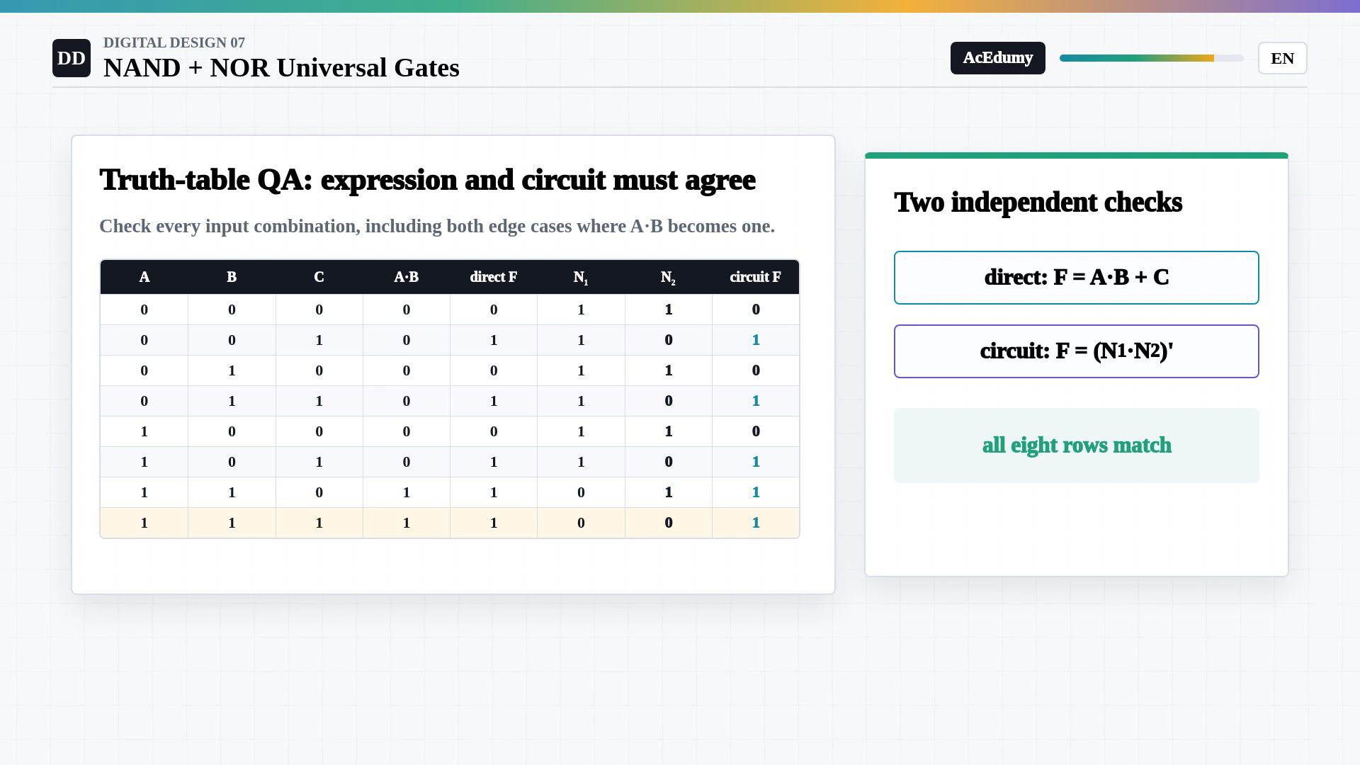
Output bubbles indicate complementation. Tied inputs share a junction; the two inputs of the final NAND in the worked circuit remain distinct. The direct expression A·B OR C and the three-NAND output agree for all eight binary assignments. Compare the circuit with the direct function for every input.Compute the direct output and each of the three NAND outputs independently.Number of input assignments:N₁ complements the product A·B; N₂ complements C; the last gate complements their product.All eight final outputs match the direct expression.With A and B both one, either value of C gives:Complete truth-table agreement proves the ideal steady Boolean function.Narration transcript
A schematic is not finished until its behavior is checked. The table compares the direct expression, A B plus C, with the three internal NAND nodes. For each of the eight input combinations, compute A B and copy C. Then N one is the complement of A B, N two is the complement of C, and the final output is NAND of those two nodes. Every final value matches the direct expression. Notice the last two rows: when A and B are both one, A B forces F to one regardless of C. This complete row-by-row agreement is the strongest QA for the circuit.
6. Review universal-gate constructions

Output bubbles indicate complementation. Tied inputs share a junction; the two inputs of the final NAND in the worked circuit remain distinct. The direct expression A·B OR C and the three-NAND output agree for all eight binary assignments. Use three recurring constructions for universal gates.Tie both NAND or NOR inputs together to obtain an inverter.Invert a NAND result again to recover AND, or a NOR result again to recover OR.Use De Morgan transformations on complete terms to stay within one gate family.A single gate family can provide a reusable set of circuit cells.The source preview introduces decoders and encoders as larger combinational blocks.Narration transcript
The universal-gate workflow has three reusable moves. Tie a gate's inputs together to create NOT. Invert a NAND or NOR result again to recover AND or OR. Then use De Morgan's law to connect complete terms while staying inside one gate family. Universal gates matter because real designs can be standardized around a small library of repeated cells. Next, we will combine gates into larger functional blocks, beginning with decoders and encoders.
Source video: Digital Design #07 | NAND and NOR as Universal Gates (4:02)