Electronics 1 · Electronics Basics
#10 Clamper circuits — DC level shifting
Shift a waveform's DC level with a capacitor and diode while preserving Vpp; solve ideal, silicon, and biased cases.
Question
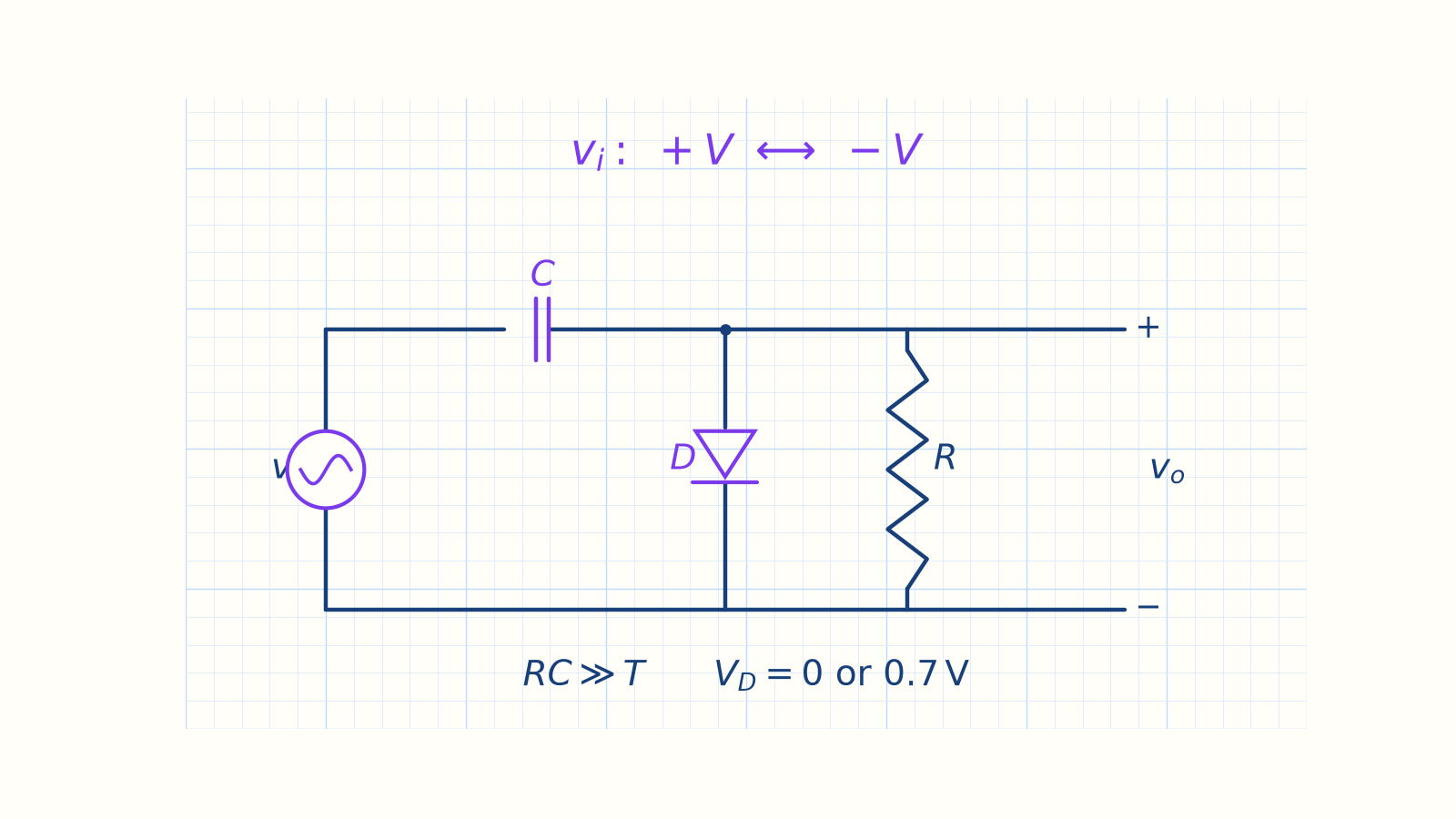
Analyze the basic series-capacitor, shunt-diode clamper for a square wave that alternates between plus V and minus V. With an ideal diode, find the charging and off states, V_C, and the output limits. Then solve the V_D = 0.7 V silicon case for a plus and minus 5 V input, followed by a biased clamper that fixes the positive peak of a plus and minus 10 V input at plus 5 V. Verify preservation of Vpp in every case.
Written solution and narration transcript(shows the full solution)
Below are all the lines written in the notebook together with the full narration transcript.
1. Clipper versus clamper
The diode charges the capacitor during one half-cycle, and the stored voltage shifts the whole waveform. Clipper → removes part of a waveformClamper → shifts the whole waveformShape and Vpp are preservedOnly the DC level changesAlso called a DC restorerNarration transcript
Welcome back. In the clipper series we learned how to cut off the peaks of a waveform. The output shape changed because part of the signal was removed. Today we start a new family of diode circuits: clampers. A clamper does something very different. It shifts the entire waveform up or down without changing its shape at all. The peak-to-peak voltage stays exactly the same. Only the DC level moves. Think of it like an elevator. A clipper is a pair of scissors that cuts the top off a building. A clamper is an elevator that moves the entire building to a different floor. This is also called a DC restorer, because it restores a known DC reference to an AC signal.
2. Basic circuit
The diode charges the capacitor during one half-cycle, and the stored voltage shifts the whole waveform. vi → series C → output voFrom output to reference: D and RLD ON → C chargesD OFF → C holds its chargeStored charge shifts the whole waveformNarration transcript
Here is the basic clamper circuit. The input signal passes through a capacitor C in series. On the output side, a diode D connects from the output node down to ground. A load resistor R sits in parallel with the diode. The capacitor is the key element. It blocks DC but passes AC. During one half-cycle the diode conducts, and the capacitor charges up to a specific voltage. During the other half-cycle the diode turns off, and the capacitor holds its charge. That stored charge adds to the input signal, shifting the entire waveform.
3. Charge and hold
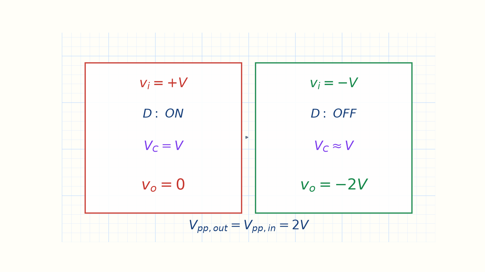
The output is clamped to zero while C charges to V; with the diode off, the output becomes minus 2V. vi = +V → D ONvi = −V → D OFFInput [−V,+V] → output [−2V,0]Narration transcript
Let us trace through the charging process step by step with an ideal diode and a square wave input of plus V to minus V. In the first half-cycle, the input is plus V. The diode is forward biased and conducts. Current flows through the diode, charging the capacitor. The capacitor charges until its voltage equals V. While the diode is on, the output is clamped to zero volts. In the second half-cycle, the input drops to minus V. Now the diode is reverse biased and turns off. No current flows, so the capacitor holds its charge at V. Apply Kirchhoff's voltage law around the loop. The output equals the input minus the capacitor voltage. That is minus V minus V, which equals minus two V. The entire waveform has shifted down by V. The input swings between plus V and minus V. The output swings between zero and minus two V. The peak-to-peak value is still two V. Nothing was cut. The shape is identical. Only the DC level changed.
4. Ideal output
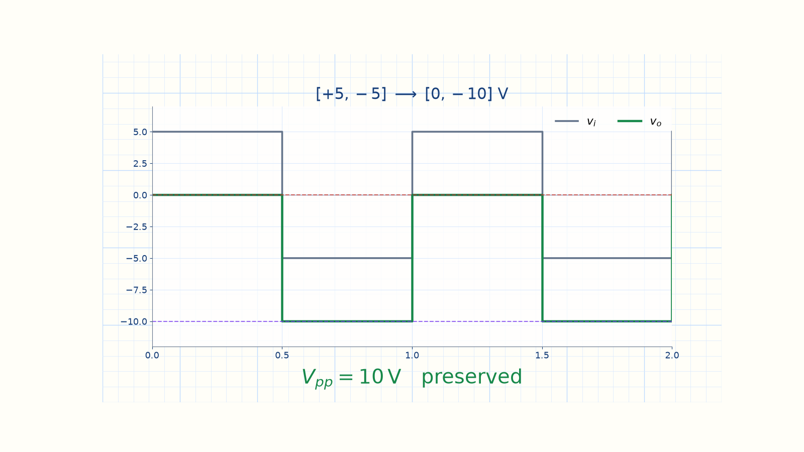
Input and output have the same peak-to-peak value; only the DC level changes. Input: +V through −VOutput: 0 through −2VShift magnitude = VC = VNarration transcript
Here is the waveform comparison. The blue curve is the input: a square wave from plus V to minus V. The green curve is the output: shifted down so the positive peak sits at zero and the negative peak sits at minus two V. Notice the peak-to-peak is preserved. The shift equals the capacitor voltage V sub C, which in this ideal case is exactly V.
5. Silicon model
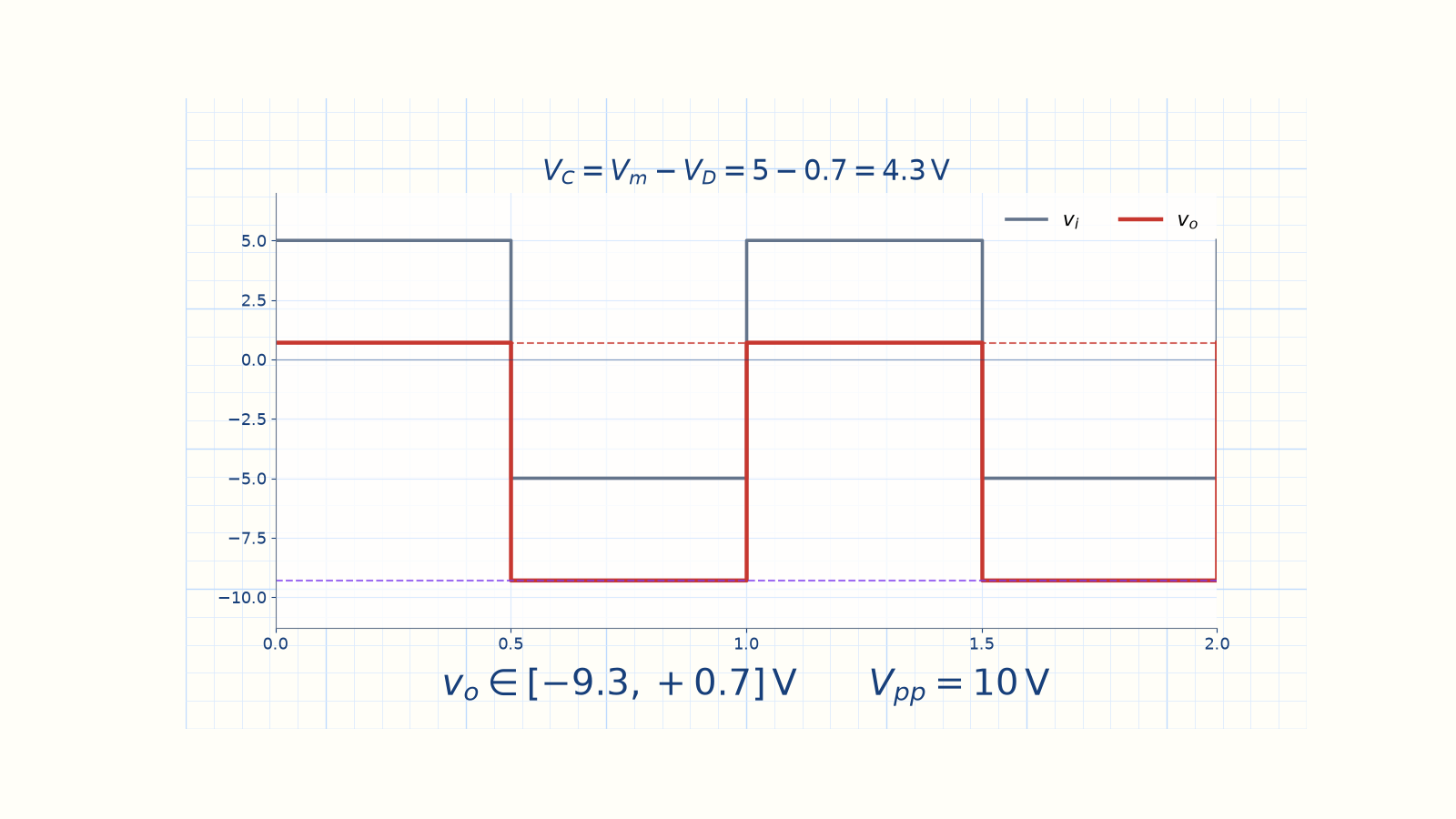
The 10 V peak-to-peak span is preserved for a plus and minus 5 V input. Narration transcript
Now let us add the silicon diode drop. The input is a square wave with a peak of five volts, swinging from plus five to minus five. The silicon diode has a forward voltage V sub d of 0.7 volts. In region one, the input is plus five volts and the diode is on. The capacitor charges to V sub m minus V sub d. That is five minus 0.7, which equals 4.3 volts. The output during this phase is not zero. It equals the diode forward voltage: plus 0.7 volts. In region two, the input drops to minus five volts and the diode turns off. The output equals the input minus the capacitor voltage. That is minus five minus 4.3, which equals minus 9.3 volts. So the output swings from plus 0.7 volts to minus 9.3 volts. The peak-to-peak is ten volts, exactly matching the input.
6. Biased clamper
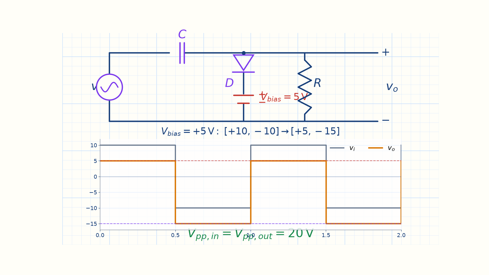
A plus and minus 10 V input shifts to plus 5 V through minus 15 V while preserving 20 Vpp. Input: +10 V through −10 VClamp reference:Output [+5,−15] V; Vpp=20 VNarration transcript
What if we want to shift the waveform to a different level, not just down to zero? We add a DC voltage source V bias in series with the diode. This is called a biased clamper. The DC source moves the reference point. Instead of clamping the positive peak to zero, we clamp it to V bias. For a clean numerical example, take a square wave that swings from plus ten to minus ten volts and set V bias to plus five volts. The diode conducts when the positive peak reaches the five volt reference, so the output maximum is plus five volts. The input has a peak-to-peak value of twenty volts, therefore the output minimum must be five minus twenty, or minus fifteen volts. The output consequently swings from plus five to minus fifteen volts. The bias source changes the DC level, while the twenty volt peak-to-peak span remains unchanged.
7. Method summary
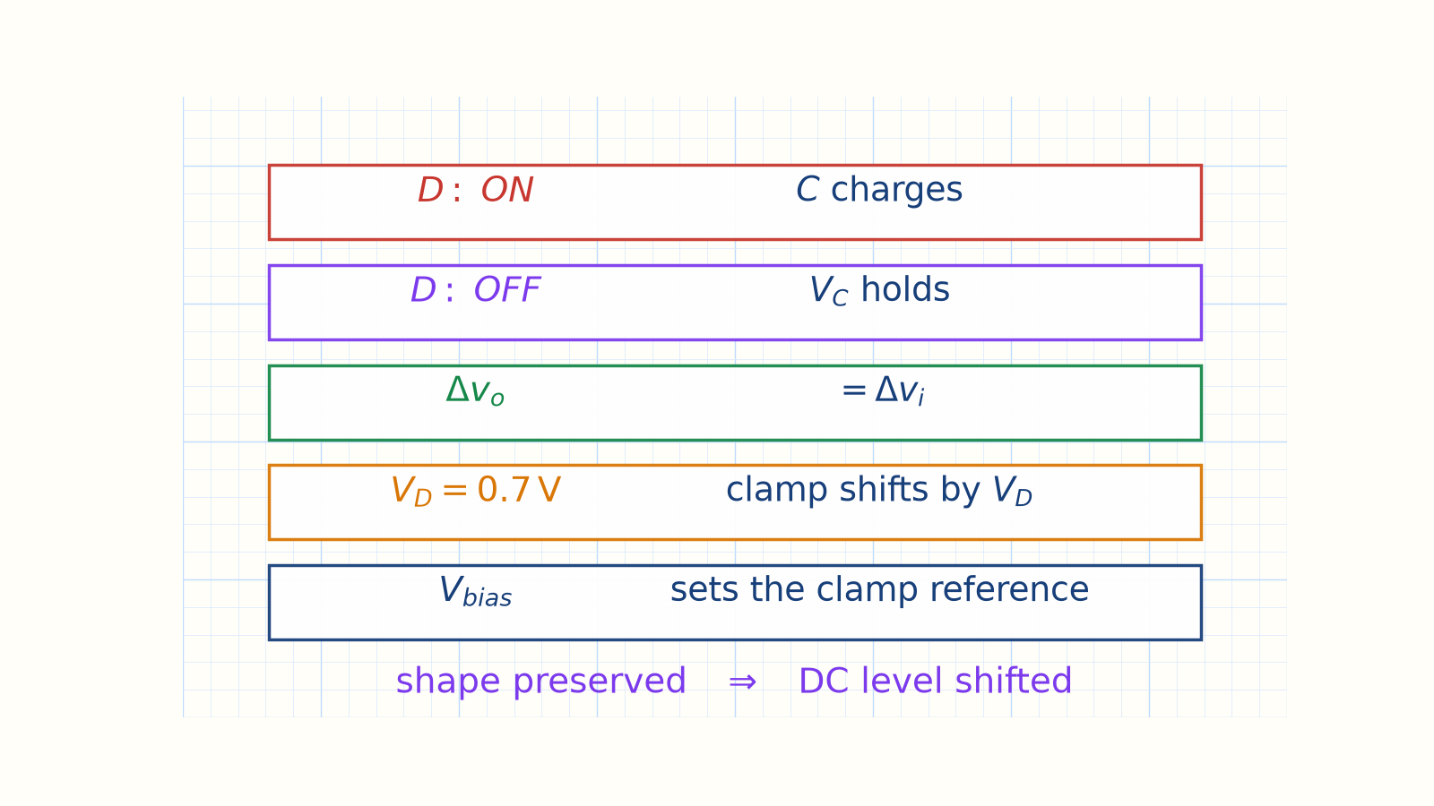
Waveform shape and Vpp are preserved in every model; only the clamp reference and DC level change. D ON charges C relative to the referenceD OFF lets VC shift the inputIdeal: a peak can clamp to 0 VSilicon: the reference moves by VDBias: the reference moves to VbiasCheck: shape and Vpp must be preservedNarration transcript
Let us review. A clamper uses a capacitor and a diode to shift the DC level of a waveform. The capacitor charges during the half-cycle when the diode conducts. That stored voltage adds to the input during the off half-cycle, creating the DC shift. With an ideal diode, the positive peak is clamped to zero. With silicon, the peak is clamped to V sub d, 0.7 volts. Adding a bias source shifts the clamp point to V bias. The key rule: peak-to-peak is always preserved. Only the DC level changes. In the next lesson, we will work through more clamper variations with different diode orientations and bias directions.
Source video: Electronics Basics #10 | Clamper Circuits: DC Level Shifting with Capacitor and Diode (5:53)