Electronics 1 · Electronics Basics
#24 Common-gate JFET bias — passing with a small margin
Question
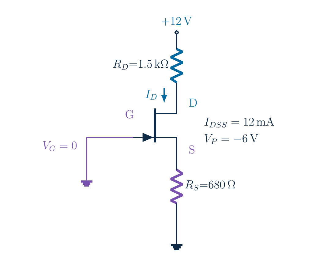
Find the DC operating point with V_DD=12 V, R_D=1.5 kΩ, R_S=680 Ω, a directly grounded gate, I_DSS=12 mA and V_P=−6 V. Distinguish V_D from V_DS, reject the invalid root, and calculate the saturation margin. This is not an AC-gain or maximum-signal-swing calculation.
Written solution and narration transcript(shows the full solution)
Below are all the lines written in the notebook together with the full narration transcript.
1. The goal: prepare a common-gate circuit
Goal: DC resting current and terminal voltagesCommon gate is the reference; no AC-gain calculation hereNarration transcript
Before discussing what a common-gate amplifier does to a signal, we must establish its DC resting condition. The goal today is to find the drain current and all the labeled voltages in this circuit. The gate is the shared reference terminal; in common-gate signal analysis the input is associated with the source and the output with the drain. Here we focus only on the bias circuit, not an AC gain calculation.
2. The goal: prepare a common-gate circuit
Gate directly grounded; no gate resistorNarration transcript
Read the original component values carefully. The drain supply is twelve volts, the drain resistor is one point five kilohms, and the source resistor is six hundred eighty ohms. That source resistance is zero point six eight kilohms. The device has I D S S of twelve milliamps and V P of negative six volts. Unlike the previous self-bias drawing, this gate has a direct ground connection, not a one-megohm gate resistor.
3. Read the grounded gate and source resistor
Ideal wire to ground → VG = 0 VNeglect gate leakage → IS ≈ IDDifferent reasons: grounded voltage and negligible gate currentNarration transcript
Use ground as the voltage reference. An ideal wire connects the gate to that reference, so the gate potential is zero volts. Separately, we neglect gate leakage in the DC model. Current conservation then makes source current approximately equal to drain current. Keep those two reasons distinct: the wire establishes gate voltage, while the negligible gate current lets us use one current through the source and drain resistors.
4. Read the grounded gate and source resistor
VGS=−0.68x V; do not mix [mA] with Ω carelesslyNarration transcript
The source resistor raises the source above ground by current times resistance. Gate-source voltage is therefore zero minus that source voltage. Define x as drain current divided by one milliamp, so x is dimensionless. Multiplying x milliamps by zero point six eight kilohms gives zero point six eight x volts. Thus gate-source voltage is negative zero point six eight x volts. Do not multiply milliamps by six hundred eighty and call the result volts without the conversion factor.
5. Form and solve the current equation
Combine bias and Shockley, assuming saturation temporarilyNarration transcript
Combine the bias relation with Shockley's equation. We are temporarily assuming saturation, so we will verify that region after calculating the drain voltage. Substitute twelve milliamps for I D S S, negative six volts for V P, and the expression for gate-source voltage. Divide by one milliamp. The negative signs in the voltage ratio cancel, giving x equals twelve times the square of one minus zero point six eight x divided by six.
6. Form and solve the current equation
Middle term: −2.72xKeep the full squared-term coefficientNarration transcript
Expand the square as one minus twice the inner term plus the inner term squared. Multiplying the middle term by twelve gives negative two point seven two x. For the squared term, twelve times zero point six eight squared divided by thirty-six gives zero point one five four one three three, continuing, times x squared. The constant term is twelve. Keep the full coefficient internally so that rounding does not distort the roots.
7. Form and solve the current equation
Move x: the linear coefficient becomes −3.72Multiply the whole equation by 0.75Narration transcript
Bring x to the right side, so negative two point seven two x becomes negative three point seven two x. We now have a quadratic equation. To make its coefficients easier to read, multiply every term by zero point seven five. This is an equivalent equation, not a different model. The result is zero point one one five six x squared, minus two point seven nine x, plus nine, equals zero. These shorter coefficients are exact for the stated component values.
8. Form and solve the current equation
Narration transcript
Use the quadratic formula. The discriminant is two point seven nine squared minus four times zero point one one five six times nine. The two terms are seven point seven eight four one and four point one six one six. Subtracting gives three point six two two five. Negative b is positive two point seven nine, and two a is zero point two three one two. The plus-or-minus sign gives two mathematical candidates.
9. Reject the root outside the device domain
Candidate 1:Candidate 2:For each root, recover VGS=−0.68x V and test its domainNarration transcript
Evaluating the minus sign gives a candidate current of approximately three point eight three five milliamps. The plus sign gives approximately twenty point three zero zero milliamps. Neither number is accepted merely because the calculator produced it. For each candidate, multiply x by negative zero point six eight to recover gate-source voltage. That voltage must belong to the physical domain of the transfer model. This is the same root-selection discipline we used in self-bias.
10. Reject the root outside the device domain
Allowed:Large root: VGS ≈ −13.804 V — rejectSmall root: VGS ≈ −2.608 V; drain check still requiredNarration transcript
The allowed gate-source interval is negative six volts through zero. The larger root would give about negative thirteen point eight zero four volts, below negative six volts, so it is invalid for this transfer model. The smaller root gives about negative two point six zero eight volts, inside the interval. Accept it as our remaining candidate, but do not yet call the whole operating point verified. The drain-source voltage still has to support saturation.
11. Find the node and terminal-pair voltages
Check the arithmetic, not an inconsistent old annotationNarration transcript
Calculate the source voltage with the accepted current. Zero point six eight kilohms times the unrounded current gives two point six zero eight volts, rounded to three decimals. The gate is at zero, so gate-source voltage is the negative of this value. One early handwritten line in the original notes had an inconsistent number; the actual multiplication and the later source-voltage result agree on about two point six zero eight. Always let the arithmetic check the annotation.
12. Find the node and terminal-pair voltages
Retain unrounded current; millivolt changes may be roundingNarration transcript
Move down from the twelve-volt supply to the drain. First find the drop across one point five kilohms. Current times resistance gives approximately five point seven five three volts. Subtract that from twelve, leaving a drain potential of approximately six point two four seven volts. Keep the current unrounded internally. If you round the current to three decimals first, the final drain voltage can shift by about one millivolt, which is only a rounding difference.
13. Find the node and terminal-pair voltages
VD ≠ VDS: ground and source are different referencesNarration transcript
Now subtract source potential from drain potential. Using the unrounded values gives a drain-source voltage of approximately three point six three nine volts. The same result comes from subtracting both resistor drops from the twelve-volt supply. Notice the distinction: the drain is about six point two four seven volts above ground, but only about three point six three nine volts above the source. Confusing these two voltages would make the saturation check misleading.
14. Saturation passes, but with a small margin
Threshold:3.639 V > 3.392 V: ideal saturation passesA pass is not a large variation/signal marginNarration transcript
Apply the saturation condition. Gate-source voltage minus V P is approximately negative two point six zero eight minus negative six, which gives three point three nine two volts. The available drain-source voltage is about three point six three nine volts, greater than the threshold. Therefore the ideal operating point passes. But the two numbers are close. Passing this inequality is not the same as having a large safety margin for component variation or signal excursion.
15. Saturation passes, but with a small margin
DC margin ≈ 3.639 − 3.392 = 0.247 VMargin = VD − VG + VPNot the maximum undistorted AC swing; signal/load analysis neededNarration transcript
Subtract the threshold from the available drain-source voltage. The difference is only about zero point two four seven volts. You can also simplify the expression to drain potential minus gate potential plus V P, which gives the same result. This is a useful DC region-consistency margin. It is not, by itself, the maximum undistorted AC output amplitude. To answer that different question, we would need a complete signal and load analysis.
16. Saturation passes, but with a small margin
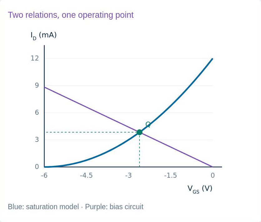
Original lesson graph; ideal DC model. Substitute in Shockley: same currentSmall nominal margin: check real tolerances and ratingsNarration transcript
Check the voltage loop: the drain-resistor drop, transistor voltage and source-resistor drop add back to twelve volts. Substitute the unrounded gate-source voltage into the transfer equation, and it returns the same current. The ideal calculation is consistent. In hardware, however, resistors and especially J FET parameters have tolerances. With such a small nominal margin, verify the actual device characteristics and ratings instead of treating the rounded classroom numbers as a guaranteed design.
17. Report a checked DC operating point
Transfer/bias intersection plus a separate drain-region checkNarration transcript
The transfer curve and source-resistor line intersect at our accepted gate-source voltage and current. That graph alone does not know whether the drain circuit has enough voltage, so we performed the separate region check. The final ideal values are about three point eight three five milliamps, with gate at zero, source at two point six zero eight, and drain at six point two four seven volts. Drain-source voltage is approximately three point six three nine volts.
18. Report a checked DC operating point
Units → valid root → voltage references → region marginNext: positive gate voltage can still give negative VGSNarration transcript
Three habits made this solution reliable: define the current units, reject roots outside the physical domain, and distinguish node voltages from voltages between terminals. Then look beyond a simple pass or fail and inspect the region margin. In the next circuit, a voltage divider will raise the gate above ground. We will see why a positive gate potential can still produce the negative gate-source voltage needed for normal n-channel J FET bias.
Source video: Electronics Basics #24 | Common-Gate JFET — DC Bias and Saturation Check (10:22)