Electronics 1 · Electronics Basics
#31 JFET and BJT shared node: quick approximation versus finite-base-current model
Question
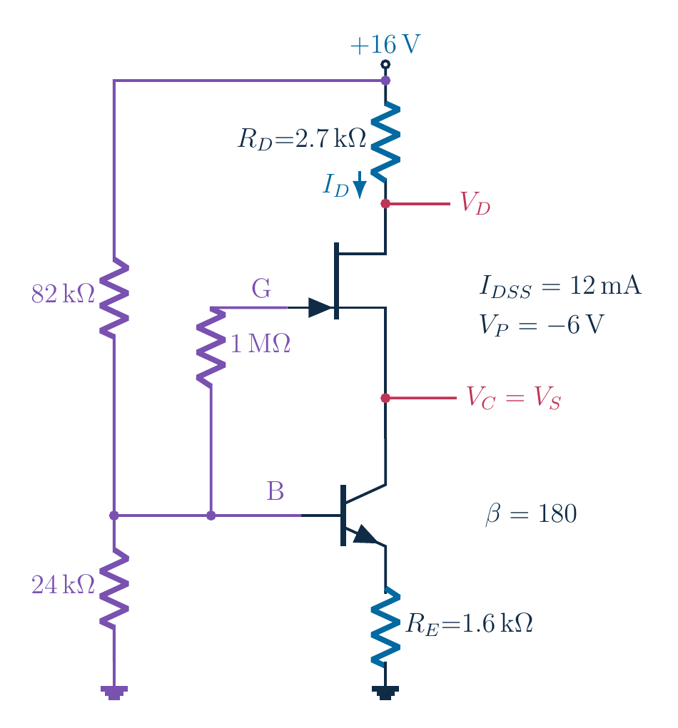
Find JFET drain voltage V_D and BJT collector voltage V_C, both relative to ground. The JFET source is the BJT collector, not emitter. Use V_DD=16 V, R_D=2.7 kΩ, R_E=1.6 kΩ, divider 82 kΩ/24 kΩ, β=180, V_BE=0.7 V, I_DSS=12 mA and V_P=−6 V. Compare unloaded and finite-base-current models.
Written solution and narration transcript(shows the full solution)
Below are all the lines written in the notebook together with the full narration transcript.
1. Start with the two voltages we want
Find ground-referenced VD and VC; JFET source = BJT collectorTwo models: quick approximation, then finite base currentNarration transcript
Before calculating, find the two red node labels on the complete circuit. We want the JFET drain voltage and the BJT collector voltage, both measured relative to ground. The collector is also the JFET source. Two different transistor models are connected through that shared node. We will solve the original problem using its quick approximation, then include the base current to see what that approximation leaves out.
2. Start with the two voltages we want
16 V; RD=2.7 kΩ; RE=1.6 kΩ; divider 82/24 kΩGate–base resistor 1 MΩ; IG≈0 → VG=VB, not VS=VENarration transcript
The supply is sixteen volts. The drain resistor is two point seven kilohms, and the emitter resistor is one point six kilohms. An eighty two and twenty four kilohm divider feeds the BJT base. The JFET gate connects to that base through one megohm. Negligible gate current means negligible drop across this one megohm resistor, so gate and base have the same voltage. It does not mean that source and emitter have the same voltage.
3. First pass: the original approximation
Approximation: unloaded divider; IC≈IENarration transcript
For the first pass, use the same approximation as the original notes: neglect divider loading and take collector current approximately equal to emitter current. The lower resistor receives twenty four out of the total one hundred and six kilohms. Multiply that fraction by sixteen volts. The unloaded base voltage is three point six two three volts. This is an approximation, not yet the base voltage with a finite base current.
4. First pass: the original approximation
Assume VBE=0.7 V; IE=(VB−0.7 V)/REApproximate IE≈IC≈ID≈1.827 [mA]Narration transcript
Assume a forward base to emitter drop of zero point seven volts. Subtract it from the unrounded base voltage to find the emitter voltage, then divide by one point six kilohms. We obtain an emitter current of one point eight two seven milliamps. In this quick approximation we also use that value for the collector and JFET drain currents. Keep extra digits in the calculation even though the screen rounds the answer.
5. Connect the JFET law to the node voltages
IDSS=12 [mA]; VP=−6 V; saturation Shockley modelID/IDSS=(1−VGS/VP)2; domain −6 V≤VGS≤0Narration transcript
Now connect the current to the JFET model. The device has a zero gate bias current of twelve milliamps and a pinch off voltage of negative six volts. Shockley’s equation relates drain current to gate to source voltage in the assumed saturation region. Dividing our current by twelve gives the squared bracket. Before taking a square root, remember the physical gate voltage interval: from negative six volts up to zero.
6. Connect the JFET law to the node voltages
Physical branch:VGS≈−3.659 V; gate below sourceNarration transcript
In that physical interval, one minus gate to source voltage divided by pinch off voltage is nonnegative. We therefore select the nonnegative square root of the current ratio. Rearranging gives gate to source voltage equal to pinch off voltage times one minus the square root. The valid value is negative three point six five nine volts. The gate is below the source, which is consistent with the reverse biased gate of this n channel JFET.
7. Connect the JFET law to the node voltages
Other root ≈ −8.341 V < −6 V: rejectSatisfying squared algebra does not establish physical conductionNarration transcript
If we expand the squared equation and solve the resulting quadratic, another root appears: about negative eight point three four one volts. Reject that second root. It lies below the negative six volt cutoff limit, where extending the squared expression would falsely predict a conducting channel again. Both roots can satisfy the algebraic square, but only one belongs to the physical conducting branch. A numerical root is not automatically an operating point.
8. Connect the JFET law to the node voltages
Shared node:Approximate VC≈7.282 V (to ground)Narration transcript
We can now find the collector voltage. Gate voltage equals base voltage, and the JFET source is the BJT collector. So gate to source voltage equals base voltage minus collector voltage. Rearrange before inserting numbers: collector voltage equals base voltage minus gate to source voltage. Subtracting a negative voltage raises the result. The approximate collector voltage is seven point two eight two volts, measured to ground.
9. Connect the JFET law to the node voltages
11.067 V from early current rounding; same approximate modelNarration transcript
For the drain node, start at the sixteen volt supply and subtract the drain resistor drop. Using the unrounded approximate current gives a drain voltage of eleven point zero six eight volts. The original notes report eleven point zero six seven because they round the current to one point eight two seven milliamps before this subtraction. That roughly one millivolt difference is rounding, not a different circuit. These are the two requested answers under the original approximation.
10. Connect the JFET law to the node voltages
JFET: VDS≈3.786 V; required boundary≈2.341 VJFET passes; VC>VB keeps BJT collector-base reverse biasedNarration transcript
Do those answers agree with the assumed operating regions? The JFET drain to source voltage is drain voltage minus collector voltage, about three point seven eight six volts. Saturation requires at least gate to source voltage minus pinch off voltage, about two point three four one volts. The inequality holds. For the BJT, collector voltage is above base voltage, keeping the collector to base junction reverse biased. The approximate solution is region consistent, though its loading assumption still needs examination.
11. Include the base current and divider loading
β=180 makes IC close to IE, not necessarily unloaded dividerSame circuit; now include IB while keeping VBE=0.7 VNarration transcript
The problem also gives a BJT current gain of one hundred and eighty. A large gain makes collector and emitter currents close, but it does not automatically make divider loading negligible. Even a small base current can create a noticeable drop through the divider’s equivalent resistance. We now keep the same physical circuit and improve only the model: include the finite base current while retaining a fixed zero point seven volt base to emitter drop.
12. Include the base current and divider loading
Narration transcript
Replace the two divider resistors by their Thevenin equivalent as viewed from the base. The open circuit voltage is the same three point six two three volts we calculated earlier. To find the equivalent resistance, short the ideal voltage supply and put eighty two and twenty four kilohms in parallel. The result is eighteen point five six six kilohms. The base current must flow through this equivalent resistance before entering the transistor.
13. Include the base current and divider loading
IB≈9.484 [μA]; microamps, not milliampsNarration transcript
Write the base loop with the emitter current expressed as beta plus one times base current. The Thevenin voltage supplies the drop across its resistance, the base to emitter drop, and the emitter resistor drop. Solving this linear equation gives a base current of nine point four eight four microamps. Notice the units: this is microamps, not milliamps. With this value the collector current can be computed without pretending it equals emitter current.
14. Include the base current and divider loading
Narration transcript
Multiply base current by one hundred and eighty. The collector and JFET drain current is now one point seven zero seven milliamps. Emitter current is slightly larger, about one point seven one seven milliamps, because it includes base current. Subtract the divider resistance drop from the Thevenin voltage to get a loaded base voltage of three point four four seven volts. The JFET gate has this same loaded voltage, because its gate current is still negligible.
15. Include the base current and divider loading
Refined VGS≈−3.737 VVD=16−ID RD≈11.391 V; finite-β modelNarration transcript
Use the same valid branch of Shockley’s equation with the refined drain current. Gate to source voltage becomes about negative three point seven three seven volts. Then subtract it from the loaded base voltage to find the collector voltage: seven point one eight four volts. Finally, subtract the drain resistor drop from sixteen volts. The drain voltage is eleven point three nine one volts. These refined values belong to the finite beta model, while the earlier pair belongs to the stated approximation.
16. Check both transistors, then compare
JFET: VDS≈4.207 V > boundary≈2.263 VBJT: VC>VB; VCE≈4.437 V; both checks passJFET saturation and BJT saturation mean different operating conditionsNarration transcript
Repeat the operating region tests with the refined values. JFET drain to source voltage is about four point two zero seven volts, above the required two point two six three volts. The collector is also above the base, and the collector to emitter voltage is about four point four three seven volts. Both region checks pass. Remember that JFET saturation means its current controlling region, while BJT saturation would be a different condition. Sharing the word does not make the two device conditions identical.
17. Check both transistors, then compare
Loading lowers VB and ID → smaller RD drop → higher VDCurrent difference about 7% relative to finite-β resultNarration transcript
Put the two solutions side by side. Divider loading lowers the base voltage and the drain current. A smaller drain current means a smaller drop across the drain resistor, so drain voltage rises. Collector voltage changes as both gate voltage and gate to source voltage change. The current difference is roughly seven percent relative to the finite beta result. The original approximation is useful, but we should identify its error before relying on it for a tighter numerical answer.
18. Check both transistors, then compare
Base network → currents → JFET voltage → requested nodesTrack shared source/collector; state assumptions; check both device regionsNarration transcript
The reusable method is to follow the dependencies, not hunt for one giant formula. Start with the base network, determine emitter and collector currents, use the JFET law to find gate to source voltage, and then recover the requested node voltages. Keep the shared source and collector node clear. State every approximation, check both operating regions, and remember that even our refined calculation still assumes an ideal gate, a fixed base to emitter drop, and simplified device laws.
Source video: Electronics Basics #31 | JFET + BJT Bias: Approximation vs Finite Beta (10:15)