Electronics 1 · Electronics Basics
#33 Common emitter: why does the output move the opposite way?
Question

Follow a small base-voltage change to the collector. Explain the inversion, then find input resistance, output resistance and voltage gain under the stated midband assumptions. Numerical values below are a supplementary teaching example, not values from the original source note.
Written solution and narration transcript(shows the full solution)
Below are all the lines written in the notebook together with the full narration transcript.
1. See the input and output first
Original source visual. Animated panels loop forward independently of the narration clock; markers show incremental signals on separate scales, not electron motion. Goal: small base signal → larger collector signal; why inverted?Signal path → local model → Rin, Rout and AvBlue input / violet output: symbolic changes around Q, separate scalesNarration transcript

Start with the goal. A small voltage signal enters the base, and we want a larger voltage signal at the collector. But when the input moves upward, the output moves downward. Why? We will follow one common emitter stage from its overall signal path to a simple model, then calculate its input resistance, output resistance and voltage gain. The blue input marker and violet output marker show changes around the operating point on separate scales. They are symbolic instruments, not moving electrons or complete measured voltages. Watch their opposite motion; we will explain it and return to the same experiment at the end.
2. See the input and output first
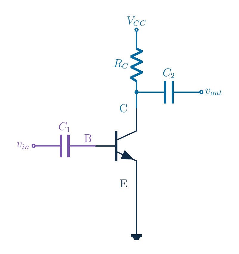
Original source visual. Animated panels loop forward independently of the narration clock; markers show incremental signals on separate scales, not electron motion. Emitter common to both ports; input at base, output at collectorBias network omitted: assume forward-active DC bias, not supplied by the capacitorNarration transcript
Now look at the original signal topology. The emitter is the common reference for both ports. Input reaches the base through the first coupling capacitor. Output leaves the collector through the second. The collector resistor goes to the supply. The drawing omits the base bias network, so it is not a complete amplifier to build as drawn. We assume that a separate bias network has already placed the transistor in forward active operation. An input capacitor alone cannot provide that direct current bias.
3. Separate the signal from the operating point
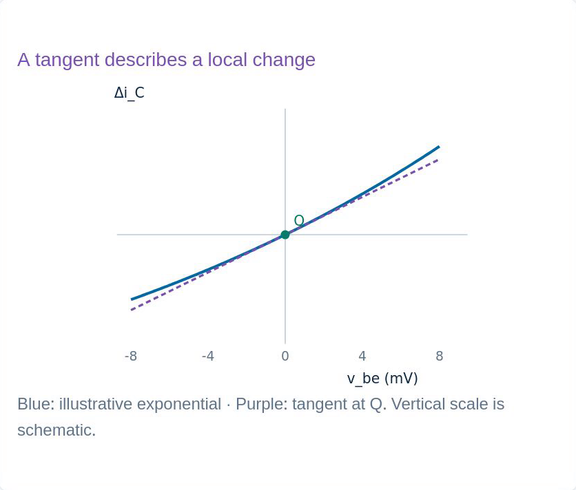
Small-signal analysis concerns changes around a DC operating pointLocal tangent ≈ curved characteristic; small signal does not mean zero biasNarration transcript
In the earlier lessons we found a direct current operating point. Small signal analysis asks a different question: how much do the currents change when the input moves slightly around that point? Write the total base emitter voltage as its bias value plus a small change. Do the same for collector current. The transistor relation is curved, but near one operating point its tangent gives a useful linear approximation. Small signal means a small excursion around that point, not a transistor with no bias.
4. Separate the signal from the operating point
Original source visual. Animated panels loop forward independently of the narration clock; markers show incremental signals on separate scales, not electron motion. Midband: coupling capacitors ≈ signal shorts; internal capacitances neglectedConstant supply → AC ground; never a physical supply shortReconsider near low/high frequency limitsNarration transcript
We use the midband model. At the frequencies of interest, the two coupling capacitors have sufficiently small impedance to approximate signal short circuits. Internal transistor capacitances are still negligible. An ideal constant supply has zero small signal variation, so its node becomes signal ground. This is a mathematical replacement in the incremental circuit. It does not mean physically shorting the power supply. Near the low frequency or high frequency limits, these simplifications must be reconsidered.
5. Replace the transistor with its local model
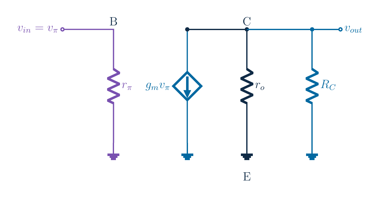
rπ between base/emitter; vπ=vin for grounded emitterControlled current: gm vπ, collector → emitterro models finite output slope; controlled source is not a batteryNarration transcript
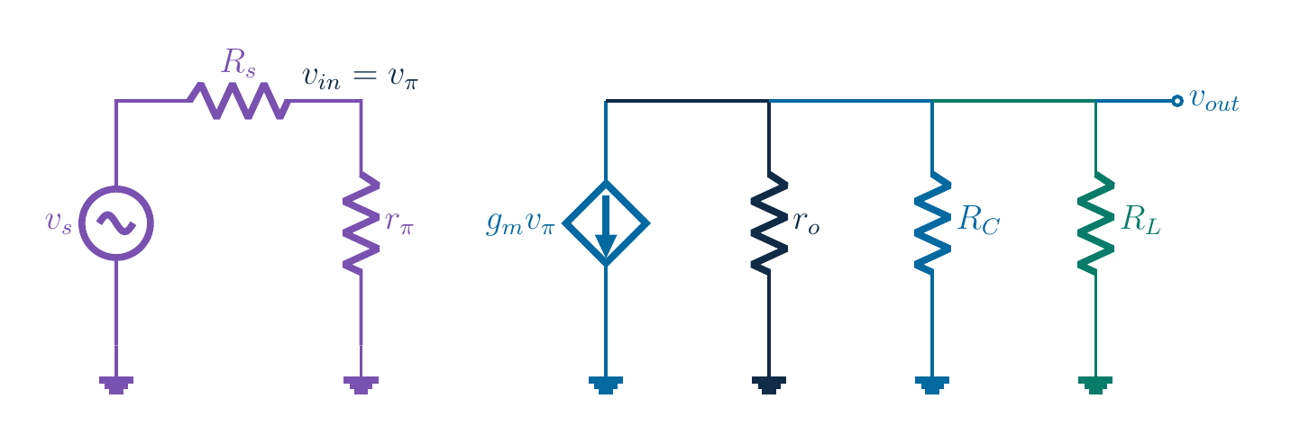
Replace the transistor with three small signal elements. Resistance r pi connects base to emitter. Its voltage is v pi, which is also the input voltage because the emitter is at signal ground. A dependent current source points from collector to emitter and has value g m times v pi. Finally, output resistance r o connects collector to emitter. This last element represents the finite slope of the collector characteristic. The dependent source is controlled by the input; it is not an extra independent battery.
6. Replace the transistor with its local model
VT≈26 [mV] is thermal voltage, not MOSFET thresholdUse the chosen DC bias current, not changing signal currentNarration transcript
The slope at the operating point is called transconductance, g m. In the usual forward active exponential model it equals the bias collector current divided by thermal voltage. Here thermal voltage is about twenty six millivolts near room temperature; it is not the MOSFET threshold from our previous lessons. Current gain beta then gives r pi equal to beta divided by g m. These parameters depend on the chosen bias point. We do not insert the changing signal current into the bias-current formula for g m.
7. Replace the transistor with its local model
Exact: gm=α/re; large β only: gm≈1/rerπ=(β+1)re≈βre; state the approximationNarration transcript
Some notes use a small emitter resistance, r e, defined as thermal voltage divided by emitter bias current. Because emitter current includes base current, alpha equals beta divided by beta plus one. The exact relation in this model is g m equals alpha divided by r e. Only when beta is large do we approximate alpha as one and write g m approximately one over r e. Similarly, r pi equals beta plus one times r e, and is only approximately beta times r e. These are compatible models when their approximations are stated.
8. Read the input and output resistances
Grounded emitter, no bias shunt, no collector-base capacitanceRestored bias network loads the input in parallelNarration transcript
Look into the input port of this simplified stage. Input current is base current, and input voltage is the voltage across r pi. Their ratio gives input resistance equal to r pi. This conclusion belongs to the circuit shown: emitter at signal ground, no explicit bias-network shunt, and no collector-to-base feedback capacitance. If we restore a real bias resistor network, that network also draws signal current and generally appears in parallel at the input. Never take this one-port result as a universal resistance of every BJT amplifier.
9. Read the input and output resistances
Remove load, zero independent input: vπ=0; dependent source vanishes hereRout=RC ∥ ro; excludes external loadNarration transcript
To find the amplifier output resistance, remove the external load and set the independent input signal to zero. In this unilateral model, that makes v pi zero, so the controlled current source becomes zero because of its controlling voltage. We have not discarded dependent sources by a general rule. A test voltage at the output now sends current through the collector resistor and r o in parallel. Therefore output resistance is their parallel combination. An external load is not included in this intrinsic output-resistance measurement.
10. Derive the sign and size of the gain
Original source visual. Animated panels loop forward independently of the narration clock; markers show incremental signals on separate scales, not electron motion. KCL at collector; currents leaving are positivevo=−gm vπ(RC ∥ ro); minus sign follows KCLNarration transcript
Now restore the input signal and apply current balance at the collector. Take currents leaving the output node as positive. The resistor currents are output voltage over collector resistance and output voltage over r o. The dependent current source also leaves the collector, with value g m times v pi. Their algebraic sum must be zero. Rearranging gives output voltage equal to negative g m times v pi times the parallel output resistance. The minus sign came from current directions, not from a memorized label on the amplifier.
11. Derive the sign and size of the gain
Original source visual. Animated panels loop forward independently of the narration clock; markers show incremental signals on separate scales, not electron motion. Input ↑ → collector current ↑ → resistor drop ↑ → output ↓Supply provides output power; amber marker is change in resistor dropNegative current CHANGE does not imply reversed total currentNarration transcript
Because v pi is the input voltage, the voltage gain is negative g m times the parallel combination of collector resistance and r o. We can also replace g m by beta over r pi. The physical picture is simple: a positive input change increases collector current; the increased resistor drop lowers the collector voltage. The output signal is inverted, or one hundred eighty degrees out of phase in this resistive midband model. The transistor does not create energy; the supply provides the power associated with the amplified output. In the three-dimensional view, the amber marker tracks the change in resistor voltage drop. These are changes around the bias point: a negative current change means less forward current, not necessarily reversed total current.
12. Derive the sign and size of the gain
Added example:gm≈38.46 mSNarration transcript
The original note contains no numerical values, so let us add a clearly labelled teaching example. Assume one milliamp of collector bias current, beta one hundred, collector resistance two kilohms, output resistance one hundred kilohms, and thermal voltage twenty six millivolts. The bias point is assumed to have adequate forward active headroom for a small signal. Dividing one milliamp by twenty six millivolts gives g m about thirty eight point four six millisiemens. Then beta divided by g m gives r pi two point six kilohms.
13. Derive the sign and size of the gain
Original source visual. Animated panels loop forward independently of the narration clock; markers show incremental signals on separate scales, not electron motion. Linear prediction; real output swing must fit its DC headroomNarration transcript
The parallel combination of two kilohms and one hundred kilohms is about one point nine six one kilohms. Multiplying it by negative transconductance gives a gain of approximately negative seventy five point four one volts per volt. A one millivolt input variation therefore produces about negative seventy five point four millivolts at the output in this linear model. This is an illustrative small signal prediction, not an exact nonlinear measurement. The output swing must still fit around the actual direct current operating voltage of a real circuit.
14. Apply the model without losing its limits
Separate loaded extension:Stage gain ≈−63.05 V/VSource divider=2.6/3.6; source-to-output gain≈−45.54 V/VNarration transcript
What changes when a real source and load are connected? An external load is in parallel with the collector resistor and r o for signal gain. A source resistance also forms an input divider with r pi. In a separate extension to our example, choose a ten kilohm load and a one kilohm source resistance. Stage gain falls to about negative sixty three point zero five. The input divider is two point six over three point six, so gain from the source itself is about negative forty five point five four. Always say which input voltage your gain refers to.
15. Apply the model without losing its limits
Original source visual. Animated panels loop forward independently of the narration clock; markers show incremental signals on separate scales, not electron motion. Valid bias first; small excursion; avoid cutoff and saturationCheck midband impedances; include actual bias, source and loadExact simplified-model relation ≠ large-β approximationNarration transcript
Keep the boundaries of the calculation visible. First establish a valid bias point, then use a small excursion so the tangent remains a useful approximation. Check that the output does not drive the transistor toward cutoff or saturation. Use the midband capacitor assumptions only where their impedances justify them. Include the bias network, source and load when the actual circuit contains them. Finally, do not erase the distinction between an exact relation inside a simplified model and an approximation such as alpha near one.
16. Apply the model without losing its limits
Answer: base signal ↑ → collector current ↑ → collector voltage ↓Bias → local model → equations; next: emitter resistanceNarration transcript
Return to the overview. A small positive base signal raises collector current and lowers collector voltage, so the common emitter stage inverts its output. Under our stated assumptions, input resistance is r pi, output resistance is the parallel collector resistance and r o, and unloaded voltage gain is negative g m times that output resistance. The workflow is bias first, local transistor model second, circuit equations third. In the next lesson an emitter resistor will change what the input sees and how strongly the stage amplifies.
Source video: Electronics Basics #33 | Common Emitter: Why Does the Output Invert? (11:04)